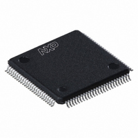
LPC1767FBD100,551 NXP Semiconductors, LPC1767FBD100,551 Datasheet - Page 12

LPC1767FBD100,551
Manufacturer Part Number
LPC1767FBD100,551
Description
IC ARM CORTEX MCU 512K 100-LQFP
Manufacturer
NXP Semiconductors
Series
LPC17xxr
Datasheets
1.LPC1767FBD100551.pdf
(2 pages)
2.LPC1767FBD100551.pdf
(840 pages)
3.LPC1767FBD100551.pdf
(65 pages)
Specifications of LPC1767FBD100,551
Core Processor
ARM® Cortex-M3™
Core Size
32-Bit
Speed
100MHz
Connectivity
Ethernet, I²C, IrDA, Microwire, SPI, SSI, UART/USART
Peripherals
Brown-out Detect/Reset, DMA, I²S, Motor Control PWM, POR, PWM, WDT
Number Of I /o
70
Program Memory Size
512KB (512K x 8)
Program Memory Type
FLASH
Ram Size
64K x 8
Voltage - Supply (vcc/vdd)
2.4 V ~ 3.6 V
Data Converters
A/D 8x12b, D/A 1x10b
Oscillator Type
Internal
Operating Temperature
-40°C ~ 85°C
Package / Case
100-LQFP
Processor Series
LPC17
Core
ARM Cortex M3
3rd Party Development Tools
MDK-ARM, RL-ARM, ULINK2, MCB1760, MCB1760U, MCB1760UME
For Use With
622-1005 - USB IN-CIRCUIT PROG ARM7 LPC2K
Lead Free Status / RoHS Status
Lead free / RoHS Compliant
Eeprom Size
-
Lead Free Status / Rohs Status
Details
Other names
568-4967
935289808551
935289808551
Available stocks
Company
Part Number
Manufacturer
Quantity
Price
Company:
Part Number:
LPC1767FBD100,551
Manufacturer:
NXP Semiconductors
Quantity:
10 000
NXP Semiconductors
Table 3.
LPC1768_67_66_65_64_3
Product data sheet
Symbol
P2[4]/PWM1[5]/
DSR1/
TRACEDATA[1]
P2[5]/PWM1[6]/
DTR1/
TRACEDATA[0]
P2[6]/PCAP1[0]/
RI1/TRACECLK
P2[7]/RD2/
RTS1
P2[8]/TD2/
TXD2
P2[9]/
USB_CONNECT/
RXD2
P2[10]/EINT0/NMI
P2[11]/EINT1/
I2STX_CLK
P2[12]/EINT2/
I2STX_WS
Pin description
Pin
69
68
67
66
65
64
53
52
51
[1]
[1]
[1]
[1]
[1]
[1]
[6]
[6]
[6]
…continued
Type
I/O
O
I
O
I/O
O
O
O
I/O
I
I
O
I/O
I
O
I/O
O
O
I/O
O
I
I/O
I
I
I/O
I
I/O
I/O
I
I/O
Description
P2[4] — General purpose digital input/output pin.
PWM1[5] — Pulse Width Modulator 1, channel 5 output.
DSR1 — Data Set Ready input for UART1.
TRACEDATA[1] — Trace data, bit 1.
P2[5] — General purpose digital input/output pin.
PWM1[6] — Pulse Width Modulator 1, channel 6 output.
DTR1 — Data Terminal Ready output for UART1. Can also be configured to be an
RS-485/EIA-485 output enable signal.
TRACEDATA[0] — Trace data, bit 0.
P2[6] — General purpose digital input/output pin.
PCAP1[0] — Capture input for PWM1, channel 0.
RI1 — Ring Indicator input for UART1.
TRACECLK — Trace Clock.
P2[7] — General purpose digital input/output pin.
RD2 — CAN2 receiver input. (LPC1768/66/65/64 only).
RTS1 — Request to Send output for UART1. Can also be configured to be an
RS-485/EIA-485 output enable signal.
P2[8] — General purpose digital input/output pin.
TD2 — CAN2 transmitter output. (LPC1768/66/65/64 only).
TXD2 — Transmitter output for UART2.
P2[9] — General purpose digital input/output pin.
USB_CONNECT — Signal used to switch an external 1.5 kΩ resistor under
software control. Used with the SoftConnect USB feature. (LPC1768/66/65/64
only).
RXD2 — Receiver input for UART2.
P2[10] — General purpose digital input/output pin.
Note: LOW on this pin while RESET is LOW forces on-chip bootloader to take
over control of the part after a reset.
EINT0 — External interrupt 0 input.
NMI — Non-maskable interrupt input.
P2[11] — General purpose digital input/output pin.
EINT1 — External interrupt 1 input.
I2STX_CLK — Transmit Clock. It is driven by the master and received by the
slave. Corresponds to the signal SCK in the I
(LPC1768/67/66/65 only).
P2[12] — General purpose digital input/output pin.
EINT2 — External interrupt 2 input.
I2STX_WS — Transmit Word Select. It is driven by the master and received by the
slave. Corresponds to the signal WS in the I
(LPC1768/67/66/65 only).
Rev. 03 — 19 November 2009
LPC1768/67/66/65/64
32-bit ARM Cortex-M3 microcontroller
2
S-bus specification.
2
S-bus specification.
© NXP B.V. 2009. All rights reserved.
12 of 65


