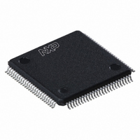
LPC1769FBD100,551 NXP Semiconductors, LPC1769FBD100,551 Datasheet - Page 54

LPC1769FBD100,551
Manufacturer Part Number
LPC1769FBD100,551
Description
IC ARM CORTEX MCU 512K 100-LQFP
Manufacturer
NXP Semiconductors
Series
LPC17xxr
Datasheets
1.OM11043.pdf
(79 pages)
2.LPC1767FBD100551.pdf
(2 pages)
3.LPC1767FBD100551.pdf
(840 pages)
4.LPC1769FBD100551.pdf
(66 pages)
Specifications of LPC1769FBD100,551
Program Memory Type
FLASH
Program Memory Size
512KB (512K x 8)
Package / Case
100-LQFP
Core Processor
ARM® Cortex-M3™
Core Size
32-Bit
Speed
120MHz
Connectivity
CAN, Ethernet, I²C, IrDA, Microwire, SPI, SSI, UART/USART, USB OTG
Peripherals
Brown-out Detect/Reset, DMA, I²S, Motor Control PWM, POR, PWM, WDT
Number Of I /o
70
Ram Size
64K x 8
Voltage - Supply (vcc/vdd)
2.4 V ~ 3.6 V
Data Converters
A/D 8x12b, D/A 1x10b
Oscillator Type
Internal
Operating Temperature
-40°C ~ 85°C
Processor Series
LPC17
Core
ARM Cortex M3
Data Bus Width
32 bit
Data Ram Size
64 KB
Interface Type
Ethernet, USB, OTG, CAN
Maximum Clock Frequency
120 MHz
Number Of Programmable I/os
70
Number Of Timers
4
Operating Supply Voltage
3.3 V
Maximum Operating Temperature
+ 85 C
Mounting Style
SMD/SMT
3rd Party Development Tools
MDK-ARM, RL-ARM, ULINK2, MCB1760, MCB1760U, MCB1760UME
Minimum Operating Temperature
- 40 C
On-chip Adc
12 bit, 8 Channel
On-chip Dac
10 bit
Lead Free Status / RoHS Status
Lead free / RoHS Compliant
For Use With
622-1005 - USB IN-CIRCUIT PROG ARM7 LPC2K
Eeprom Size
-
Lead Free Status / Rohs Status
Lead free / RoHS Compliant
Other names
568-4966
935290522551
935290522551
Available stocks
Company
Part Number
Manufacturer
Quantity
Price
Company:
Part Number:
LPC1769FBD100,551
Manufacturer:
NXP Semiconductors
Quantity:
10 000
NXP Semiconductors
12. ADC electrical characteristics
Table 16.
V
[1]
[2]
[3]
[4]
[5]
[6]
[7]
[8]
LPC1769_68_67_66_65_64_4
Product data sheet
Symbol
V
C
E
E
E
E
E
R
f
f
clk(ADC)
c(ADC)
DDA
IA
D
L(adj)
O
G
T
ia
vsi
Conditions: V
The ADC is monotonic, there are no missing codes.
The differential linearity error (E
The integral non-linearity (E
appropriate adjustment of gain and offset errors. See
The offset error (E
ideal curve. See
The gain error (E
error, and the straight line which fits the ideal transfer curve. See
The absolute error (E
ADC and the ideal transfer curve. See
See
= 2.7 V to 3.6 V; T
Figure
ADC characteristics
Parameter
analog input voltage
analog input capacitance
differential linearity error
integral non-linearity
offset error
gain error
absolute error
voltage source interface
resistance
ADC clock frequency
ADC conversion frequency
22.
SSA
Figure
G
= 0 V, V
O
) is the relative difference in percent between the straight line fitting the actual transfer curve after removing offset
) is the absolute difference between the straight line which fits the actual curve and the straight line which fits the
T
amb
) is the maximum difference between the center of the steps of the actual transfer curve of the non-calibrated
21.
Fig 20.
DDA
=
L(adj)
−
= 3.3 V.
40
D
) is the peak difference between the center of the steps of the actual and the ideal transfer curve after
) is the difference between the actual step width and the ideal step width. See
°
C to +85
SPI slave timing (CPHA = 0)
Figure
SCK (CPOL = 0)
SCK (CPOL = 1)
Conditions
°
21.
C unless otherwise specified; ADC frequency 13 MHz.
MOSI
MISO
Rev. 04 — 1 February 2010
Figure
21.
Figure
DATA VALID
DATA VALID
t
SPIQV
LPC1769/68/67/66/65/64
21.
[1][2][3]
[1][4]
[1][5]
[1][6]
[1][7]
[8]
T
SPICYC
Min
0
-
-
-
-
-
-
-
-
-
t
32-bit ARM Cortex-M3 microcontroller
SPIDSU
DATA VALID
DATA VALID
t
SPICLKH
t
Typ
-
-
-
-
±2
-
-
-
-
-
SPIDH
t
SPICLKL
t
002aad989
SPIOH
Max
V
15
±1
±3
-
0.5
4
7.5
13
200
Figure
© NXP B.V. 2010. All rights reserved.
DDA
21.
Unit
V
pF
LSB
LSB
LSB
%
LSB
kΩ
MHz
kHz
54 of 66


