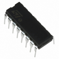
ST7FLIT19BY1B6 STMicroelectronics, ST7FLIT19BY1B6 Datasheet - Page 149

ST7FLIT19BY1B6
Manufacturer Part Number
ST7FLIT19BY1B6
Description
IC MCU 8BIT 4K FLASH 16DIP
Manufacturer
STMicroelectronics
Series
ST7r
Datasheet
1.ST7FLIT15BY1M6.pdf
(159 pages)
Specifications of ST7FLIT19BY1B6
Core Processor
ST7
Core Size
8-Bit
Speed
8MHz
Connectivity
SPI
Peripherals
LVD, POR, PWM, WDT
Number Of I /o
13
Program Memory Size
4KB (4K x 8)
Program Memory Type
FLASH
Eeprom Size
128 x 8
Ram Size
256 x 8
Voltage - Supply (vcc/vdd)
2.7 V ~ 5.5 V
Data Converters
A/D 7x10b
Oscillator Type
Internal
Operating Temperature
-40°C ~ 85°C
Package / Case
16-DIP (0.300", 7.62mm)
Processor Series
ST7FLIT1x
Core
ST7
Data Bus Width
8 bit
Data Ram Size
256 B
Interface Type
SPI
Maximum Clock Frequency
8 MHz
Number Of Programmable I/os
17
Number Of Timers
4
Maximum Operating Temperature
+ 85 C
Mounting Style
Through Hole
Development Tools By Supplier
ST7FLITE-SK/RAIS, ST7FLIT1B-D/RAIS, ST7MDT10-DVP3, ST7MDT10-EMU3, STX-RLINK
Minimum Operating Temperature
- 40 C
On-chip Adc
10 bit, 7 Channel
For Use With
497-6232 - BOARD EVAL ST7LITE1B,STP5NK60Z497-5049 - KIT STARTER RAISONANCE ST7FLITE497-5046 - KIT TOOL FOR ST7/UPSD/STR7 MCU
Lead Free Status / RoHS Status
Lead free / RoHS Compliant
Other names
497-5629-5
Available stocks
Company
Part Number
Manufacturer
Quantity
Price
Company:
Part Number:
ST7FLIT19BY1B6
Manufacturer:
ALTERA
Quantity:
101
15 DEVICE CONFIGURATION AND ORDERING INFORMATION
Each device is available for production in user pro-
grammable versions (FLASH).
15.1 OPTION BYTES
The two option bytes allow the hardware configu-
ration of the microcontroller to be selected.
The option bytes can be accessed only in pro-
gramming mode (for example using a standard
ST7 programming tool).
OPTION BYTE 0
OPT7 = Reserved, must always be 1.
OPT6 = PKG Package selection
0: 16-pin package
1: 20-pin package
OPT5:4 = CLKSEL Clock Source Selection
When the internal RC oscillator is not selected
(Option OSC=1), these option bits select the clock
source: resonator oscillator or external clock
Note: When the internal RC oscillator is selected,
the CLKSEL option bits must be kept at their de-
fault value in order to select the 256 clock cycle
delay (see
Default
Resonator
Ext.
Clock source:
CLKIN
Value
Clock Source
Reserved
Res. PKG
7
1
Section
on PB4
on PC0
1
7.5).
CLKSEL
1
Ext. Osc Disabled/
Ext. Osc Enabled/
OPTION BYTE 0
Port C Disabled
Port C Enabled
1
Port C
SEC1 SEC0
0
1
CLKSEL
0
0
1
1
FMP
R
0
0
1
1
0
FMP
W
0
0
ST7FLITE1xB devices are shipped to customers
with a default program memory content (FFh).
This implies that FLASH devices have to be con-
figured by the customer using the Option Bytes.
OPT3:2 = SEC[1:0] Sector 0 size definition
These option bits indicate the size of sector 0 ac-
cording to the following table.
OPT1 = FMP_R Read-out protection
Readout protection, when selected provides a pro-
tection against program memory content extrac-
tion and against write access to Flash memory.
Erasing the option bytes when the FMP_R option
is selected will cause the whole memory to be
erased first and the device can be reprogrammed.
Refer to the ST7 Flash Programming Reference
Manual and
tails
0: Read-out protection off
1: Read-out protection on
OPT0 = FMP_W FLASH write protection
This option indicates if the FLASH program mem-
ory is write protected.
Warning: When this option is selected, the pro-
gram memory (and the option bit itself) can never
be erased or programmed again.
0: Write protection off
1: Write protection on
Sector 0 Size
x4x8
PLL
1
7
0.5k
1k
2k
4k
OFF
PLL
1
section 4.5 on page 14
PLL32
OFF
1
OPTION BYTE 1
SEC1
OSC LVD1 LVD0
0
0
1
1
0
1
1
ST7LITE1xB
for more de-
SEC0
WDG
SW
1
0
1
0
1
149/159
HALT
WDG
0
1


