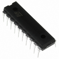
ST7FLITE25F2B6 STMicroelectronics, ST7FLITE25F2B6 Datasheet - Page 48

ST7FLITE25F2B6
Manufacturer Part Number
ST7FLITE25F2B6
Description
IC MCU 8BIT 8K FLASH 20DIP
Manufacturer
STMicroelectronics
Series
ST7r
Datasheet
1.ST7FLITE20F2B6.pdf
(133 pages)
Specifications of ST7FLITE25F2B6
Core Processor
ST7
Core Size
8-Bit
Speed
8MHz
Connectivity
SPI
Peripherals
LVD, POR, PWM, WDT
Number Of I /o
15
Program Memory Size
8KB (8K x 8)
Program Memory Type
FLASH
Ram Size
384 x 8
Voltage - Supply (vcc/vdd)
2.4 V ~ 5.5 V
Data Converters
A/D 7x10b
Oscillator Type
Internal
Operating Temperature
-40°C ~ 85°C
Package / Case
20-DIP (0.300", 7.62mm)
Processor Series
ST7FLITE2x
Core
ST7
Data Bus Width
8 bit
Data Ram Size
384 B
Interface Type
SPI
Maximum Clock Frequency
8 MHz
Number Of Programmable I/os
15
Number Of Timers
4 bit
Operating Supply Voltage
2.4 V to 5.5 V
Maximum Operating Temperature
+ 85 C
Mounting Style
Through Hole
Development Tools By Supplier
ST7FLIT2-COS/COM, ST7FLITE-SK/RAIS, ST7MDT10-DVP3, ST7MDT10-EMU3, STX-RLINK
Minimum Operating Temperature
- 40 C
On-chip Adc
13 bit
For Use With
497-5858 - EVAL BOARD PLAYBACK ST7FLITE497-5049 - KIT STARTER RAISONANCE ST7FLITE
Lead Free Status / RoHS Status
Lead free / RoHS Compliant
Eeprom Size
-
Lead Free Status / Rohs Status
In Transition
Other names
497-4858
Available stocks
Company
Part Number
Manufacturer
Quantity
Price
ST7LITE2
I/O PORTS (Cont’d)
Figure 31. I/O Port General Block Diagram
Table 8. I/O Port Mode Options
Legend: NI - not implemented
48/133
1
Input
Output
REGISTER
ACCESS
INTERRUPT
REQUEST (ei
EXTERNAL
Off - implemented not activated
On - implemented and activated
DDR SEL
OR SEL
DR SEL
Floating with/without Interrupt
Pull-up with/without Interrupt
Push-pull
Open Drain (logic level)
True Open Drain
Configuration Mode
DDR
DR
OR
x
)
SENSITIVITY
SELECTION
ALTERNATE
OUTPUT
From on-chip periphera
ALTERNATE
ENABLE
BIT
If implemented
1
0
Combinational
Logic
l
1
0
FROM
OTHER
BITS
Pull-Up
Note: Refer to the Port Configuration
table for device specific information.
Off
On
Off
NI
Note: The diode to V
true open drain pads. A local protection between
the pad and V
vice against positive stress.
N-BUFFER
PULL-UP
CONDITION
P-Buffer
Off
On
Off
NI
OL
SCHMITT
TRIGGER
CMOS
is implemented to protect the de-
V
DD
DD
NI (see note)
is not implemented in the
to V
On
DD
P-BUFFER
(see table below)
To on-chip peripheral
V
Diodes
DD
DIODES
(see table below)
PULL-UP
(see table below)
ALTERNATE
ANALOG
INPUT
to V
INPUT
PAD
On
SS


