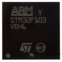
STM32F103VBH6 STMicroelectronics, STM32F103VBH6 Datasheet - Page 55

STM32F103VBH6
Manufacturer Part Number
STM32F103VBH6
Description
MCU ARM 128KB FLASH MEM 100-LFBG
Manufacturer
STMicroelectronics
Series
STM32r
Datasheet
1.STM32F103V8H6.pdf
(67 pages)
Specifications of STM32F103VBH6
Core Processor
ARM® Cortex-M3™
Core Size
32-Bit
Speed
72MHz
Connectivity
CAN, I²C, IrDA, LIN, SPI, UART/USART, USB
Peripherals
DMA, Motor Control PWM, PDR, POR, PVD, PWM, Temp Sensor, WDT
Number Of I /o
80
Program Memory Size
128KB (128K x 8)
Program Memory Type
FLASH
Ram Size
20K x 8
Voltage - Supply (vcc/vdd)
2 V ~ 3.6 V
Data Converters
A/D 16x12b
Oscillator Type
Internal
Operating Temperature
-40°C ~ 85°C
Package / Case
100-LFBGA
Processor Series
STM32F103x
Core
ARM Cortex M3
Data Bus Width
32 bit
Data Ram Size
20 KB
Interface Type
CAN, I2C, SPI, USART, USB
Maximum Clock Frequency
72 MHz
Number Of Programmable I/os
100
Number Of Timers
3 x 16 bit
Operating Supply Voltage
2 V to 3.6 V
Maximum Operating Temperature
+ 105 C
Mounting Style
SMD/SMT
3rd Party Development Tools
EWARM, EWARM-BL, MDK-ARM, RL-ARM, ULINK2
Development Tools By Supplier
ST-LINK
Minimum Operating Temperature
- 40 C
On-chip Adc
12 bit x 2, 16 Channel
For Use With
497-10048 - BOARD EVAL ACCELEROMETER497-10030 - STARTER KIT FOR STM32497-9091 - LED BOARD FOR STM32 STP16DP05497-8853 - BOARD DEMO STM32 UNIV USB-UUSCIKSDKSTM32-PL - KIT IAR KICKSTART STM32 CORTEXM3497-8512 - KIT STARTER FOR STM32F10XE MCU497-8511 - KIT STARTER FOR STM32 512K FLASH497-8505 - KIT STARTER FOR STM32F10XE MCU497-8304 - KIT STM32 MOTOR DRIVER BLDC497-6438 - BOARD EVALUTION FOR STM32 512K497-6289 - KIT PERFORMANCE STICK FOR STM32MCBSTM32UME - BOARD EVAL MCBSTM32 + ULINK-MEMCBSTM32U - BOARD EVAL MCBSTM32 + ULINK2MCBSTM32 - BOARD EVAL FOR STM STM32X SER497-6053 - KIT STARTER FOR STM32497-6052 - KIT STARTER FOR STM32497-6050 - KIT STARTER FOR STM32497-6049 - KIT EVALUATION LOW COST STM32497-6048 - BOARD EVALUATION FOR STM32497-6047 - KIT DEVELOPMENT FOR STM32497-5046 - KIT TOOL FOR ST7/UPSD/STR7 MCU
Lead Free Status / RoHS Status
Lead free / RoHS Compliant
Eeprom Size
-
Lead Free Status / Rohs Status
Details
Other names
497-6069
Available stocks
Company
Part Number
Manufacturer
Quantity
Price
Company:
Part Number:
STM32F103VBH6
Manufacturer:
STMicroelectronics
Quantity:
135
Company:
Part Number:
STM32F103VBH6
Manufacturer:
EVERLIGHT
Quantity:
30
Part Number:
STM32F103VBH6
Manufacturer:
ST
Quantity:
20 000
STM32F103xx
Table 39.
1. TBD = to be determined.
2. Depending on the input signal variation (f
3. During the sample time the input capacitance C
Table 40.
1. TBD = to be determined.
2. ADC Accuracy vs. Negative Injection Current: Injecting negative current on any of the standard (non-
Symbol
Symbol
t
R
C
t
R
C
CONV
t
STAB
|E
|E
|E
|E
|E
I
CAL
allow the use of a larger serial resistor (R
source. The internal resistance of the analog source must allow the capacitance to reach its final voltage
level within t
the conversion result. Values for the sample clock t
robust) analog input pins should be avoided as this significantly reduces the accuracy of the conversion
being performed on another analog input. It is recommended to add a Schottky diode (pin to ground) to
standard analog pins which may potentially inject negative current.
Any positive injection current within the limits specified for I
affect the ADC accuracy.
t
ADC
ADC
t
lkg
AIN
AIN
lat
S
O
G
D
T
L
|
|
|
|
|
External input impedance
External capacitor on analog
input
Negative input leakage current
on analog pins
Sampling switch resistance
Internal sample and hold
capacitor
Calibration time
Injection conversion latency
Sampling time
Power-up time
Total conversion time (including
sampling time)
Total unadjusted error
Offset error
Gain Error
Differential linearity error
Integral linearity error
ADC characteristics
ADC accuracy (f
3.3 V)
S.
After the end of the sample time t
Parameter
(1)
(2)
Parameter
(2)
(2)
(2)
PCLK2
(2)
(1)
AIN
AIN
= 14 MHz, f
(continued)
), C
). It is valid for all f
V
on adjacent analog pin
IN
AIN
AIN
S
<
, changes of the analog input voltage have no effect on
f
f
f
V
f
S
(5 max) can be charged/discharged by the external
ADC
ADC
ADC
can be increased for stabilization time and reduced to
ADC
Conditions
SS,
depend on programming.
Conditions
= 14 MHz
= 14 MHz
= 14 MHz
| I
ADC
= 14MHz
INJ(PIN)
IN
| < 400 µA
= 14 MHz, R
ADC
and ΣI
frequencies ≤ 14 MHz.
INJ(PIN)
14 (1.5 for sampling
+12.5 for successive
approximation)
0.107
Min
Electrical characteristics
0
1
AIN
in
Typ
3
1
2
3
2
Section 5.3.12
TBD
<10 kΩ , V
0
Typ
5.9
83
5
(2)(3)
Max
TBD
TBD
TBD
TBD
TBD
0.214
3
17.1
1
18
Max
DDA
6
1
5
does not
=
1/f
1/f
1/f
Unit
LSB
Unit
kΩ
pF
µA
kΩ
pF
µs
µs
µs
µs
µs
55/67
ADC
ADC
ADC


