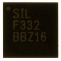
C8051F332-GM Silicon Laboratories Inc, C8051F332-GM Datasheet - Page 96

C8051F332-GM
Manufacturer Part Number
C8051F332-GM
Description
IC 8051 MCU 4KB FLASH 20QFN
Manufacturer
Silicon Laboratories Inc
Series
C8051F33xr
Specifications of C8051F332-GM
Program Memory Type
FLASH
Program Memory Size
4KB (4K x 8)
Package / Case
20-QFN
Core Processor
8051
Core Size
8-Bit
Speed
25MHz
Connectivity
SMBus (2-Wire/I²C), SPI, UART/USART
Peripherals
POR, PWM, Temp Sensor, WDT
Number Of I /o
17
Ram Size
768 x 8
Voltage - Supply (vcc/vdd)
2.7 V ~ 3.6 V
Data Converters
A/D 16x10b
Oscillator Type
Internal
Operating Temperature
-40°C ~ 85°C
Processor Series
C8051F3x
Core
8051
Data Bus Width
8 bit
Data Ram Size
768 B
Interface Type
I2C/SMBus/SPI/UART
Maximum Clock Frequency
25 MHz
Number Of Programmable I/os
17
Number Of Timers
4
Operating Supply Voltage
2.7 V to 3.6 V
Maximum Operating Temperature
+ 85 C
Mounting Style
SMD/SMT
3rd Party Development Tools
KSK-SL-TOOLSTICK, PK51, CA51, A51, ULINK2
Development Tools By Supplier
C8051F330DK
Minimum Operating Temperature
- 40 C
On-chip Adc
16-ch x 10-bit
No. Of I/o's
17
Ram Memory Size
768Byte
Cpu Speed
25MHz
No. Of Timers
4
Rohs Compliant
Yes
Package
20QFN
Device Core
8051
Family Name
C8051F33x
Maximum Speed
25 MHz
Lead Free Status / RoHS Status
Lead free / RoHS Compliant
For Use With
770-1006 - ISP 4PORT FOR SILABS C8051F MCU336-1451 - ADAPTER PROGRAM TOOLSTICK F330
Eeprom Size
-
Lead Free Status / Rohs Status
Lead free / RoHS Compliant
Other names
336-1266
Available stocks
Company
Part Number
Manufacturer
Quantity
Price
Company:
Part Number:
C8051F332-GM
Manufacturer:
Silicon Laboratories Inc
Quantity:
135
Part Number:
C8051F332-GMR
Manufacturer:
SILICON LABS/èٹ¯ç§‘
Quantity:
20 000
Important Note: The V
V
dure for configuring the V
See Figure 10.2 for V
See Table 10.1 for complete electrical characteristics of the V
10.3. External Reset
The external RST pin provides a means for external circuitry to force the device into a reset state. Assert-
ing an active-low signal on the RST pin generates a reset; an external pullup and/or decoupling of the RST
pin may be necessary to avoid erroneous noise-induced resets. See Table 10.1 for complete RST pin
specifications. The PINRSF flag (RSTSRC.0) is set on exit from an external reset.
10.4. Missing Clock Detector Reset
The Missing Clock Detector (MCD) is a one-shot circuit that is triggered by the system clock. If the system
clock remains high or low for more than 100 µs, the one-shot will time out and generate a reset. After a
MCD reset, the MCDRSF flag (RSTSRC.2) will read ‘1’, signifying the MCD as the reset source; otherwise,
this bit reads ‘0’. Writing a ‘1’ to the MCDRSF bit enables the Missing Clock Detector; writing a ‘0’ disables
it. The state of the RST pin is unaffected by this reset.
DD
Bit7:
Bit6:
Bits5–0: Reserved. Read = 000000b. Write = don’t care.
VDMEN
monitor as a reset source before it is enabled and stabilized may cause a system reset. The proce-
R/W
Bit7
Step 1. Enable the V
Step 2. Wait for the V
Step 3. Select the V
VDMEN: V
This bit turns the V
until it is also selected as a reset source in register RSTSRC (SFR Definition 10.2). The V
Monitor must be allowed to stabilize before it is selected as a reset source. Selecting the
V
See Table 10.1 for the minimum V
0: V
1: V
V
This bit indicates the current power supply status (V
0: V
1: V
DD
DD
VDDSTAT Reserved Reserved Reserved Reserved Reserved Reserved
DD
DD
DD
DD
monitor as a reset source before it has stabilized may generate a system reset.
STAT: V
Bit6
R
Monitor Disabled.
Monitor Enabled.
is at or below the V
is above the V
SFR Definition 10.1. VDM0CN: V
DD
DD
DD
monitor timing; note that the reset delay is not incurred after a V
DD
DD
Monitor Enable.
monitor must be enabled before it is selected as a reset source. Selecting the
Status.
monitor as a reset source is shown below:
DD
DD
Bit5
DD
R
DD
monitor as a reset source (PORSF bit in RSTSRC = ‘1’).
monitor (VDMEN bit in VDM0CN = ‘1’).
monitor to stabilize (see Table 10.1 for the V
DD
monitor circuit on/off. The V
monitor threshold.
DD
Bit4
R
monitor threshold.
DD
Rev. 1.7
Monitor turn-on time.
Bit3
R
DD
DD
DD
C8051F330/1/2/3/4/5
Bit2
DD
R
monitor.
Monitor cannot generate system resets
Monitor Control
Monitor output).
Bit1
R
DD
Monitor turn-on time).
SFR Address:
Bit0
R
DD
monitor reset.
0xFF
Reset Value
Variable
DD
99


