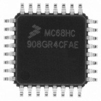
MC68HC908GR4CFAE Freescale Semiconductor, MC68HC908GR4CFAE Datasheet - Page 115

MC68HC908GR4CFAE
Manufacturer Part Number
MC68HC908GR4CFAE
Description
IC MCU 4K FLASH 8.2MHZ 32-LQFP
Manufacturer
Freescale Semiconductor
Series
HC08r
Specifications of MC68HC908GR4CFAE
Core Processor
HC08
Core Size
8-Bit
Speed
8MHz
Connectivity
SCI, SPI
Peripherals
LVD, POR, PWM
Number Of I /o
21
Program Memory Size
4KB (4K x 8)
Program Memory Type
FLASH
Ram Size
384 x 8
Voltage - Supply (vcc/vdd)
2.7 V ~ 5.5 V
Data Converters
A/D 6x8b
Oscillator Type
Internal
Operating Temperature
-40°C ~ 85°C
Package / Case
32-LQFP
Controller Family/series
HC08
No. Of I/o's
21
Ram Memory Size
1KB
Cpu Speed
8MHz
No. Of Timers
1
Embedded Interface Type
I2C, SCI, SPI
Rohs Compliant
Yes
Processor Series
HC08G
Core
HC08
Data Bus Width
8 bit
Data Ram Size
384 B
Interface Type
SCI, SPI
Maximum Clock Frequency
8 MHz
Number Of Programmable I/os
21
Number Of Timers
3
Operating Supply Voltage
3 V to 5 V
Maximum Operating Temperature
+ 125 C
Mounting Style
SMD/SMT
Development Tools By Supplier
FSICEBASE, DEMO908GZ60E, M68CBL05CE, M68EML08GPGTE
Minimum Operating Temperature
- 40 C
On-chip Adc
8 bit, 6 Channel
Lead Free Status / RoHS Status
Lead free / RoHS Compliant
Eeprom Size
-
Lead Free Status / Rohs Status
Details
Available stocks
Company
Part Number
Manufacturer
Quantity
Price
Company:
Part Number:
MC68HC908GR4CFAE
Manufacturer:
Freescale Semiconductor
Quantity:
10 000
- Current page: 115 of 408
- Download datasheet (4Mb)
7.6.1 PLL Control Register
MC68HC908GR8 — Rev 4.0
MOTOROLA
NOTES:
$003A
$003B
1. When AUTO = 0, PLLIE is forced clear and is read-only.
2. When AUTO = 0, PLLF and LOCK read as clear.
3. When AUTO = 1, ACQ is read-only.
4. When PLLON = 0 or VRS7:VRS0 = $0, BCS is forced clear and is read-only.
5. When PLLON = 1, the PLL programming register is read-only.
6. When BCS = 1, PLLON is forced set and is read-only.
Select Register (PMDS)
PLL VCO Select Range
PLL Reference Divider
Register (PMRS)
Address:
The PLL control register (PCTL) contains the interrupt enable and flag
bits, the on/off switch, the base clock selector bit, the prescaler bits, and
the VCO power-of-two range selector bits.
PLLIE — PLL Interrupt Enable Bit
Reset:
Reset:
Reset:
Read:
Read:
Read:
Write:
Write:
Write:
Figure 7-3. CGMC I/O Register Summary
Freescale Semiconductor, Inc.
This read/write bit enables the PLL to generate an interrupt request
when the LOCK bit toggles, setting the PLL flag, PLLF. When the
AUTO bit in the PLL bandwidth control register (PBWC) is clear,
PLLIE cannot be written and reads as logic 0. Reset clears the PLLIE
bit.
For More Information On This Product,
$0036
PLLIE
VRS7
Bit 7
0
0
0
0
Clock Generator Module (CGMC)
Go to: www.freescale.com
Figure 7-4. PLL Control Register (PCTL)
= Unimplemented
= Unimplemented
VRS6
PLLF
1
0
0
6
0
PLLON
VRS5
0
0
0
5
1
VRS4
BCS
R
0
0
0
4
0
= Reserved
RDS3
VRS3
PRE1
0
0
3
0
Clock Generator Module (CGMC)
RDS2
VRS2
PRE0
0
0
2
0
RDS1
CGMC Registers
VRS1
VPR1
0
0
1
0
Technical Data
RDS0
VRS0
VPR0
Bit 0
0
1
0
115
Related parts for MC68HC908GR4CFAE
Image
Part Number
Description
Manufacturer
Datasheet
Request
R
Part Number:
Description:
Manufacturer:
Freescale Semiconductor, Inc
Datasheet:
Part Number:
Description:
Manufacturer:
Freescale Semiconductor, Inc
Datasheet:
Part Number:
Description:
Manufacturer:
Freescale Semiconductor, Inc
Datasheet:
Part Number:
Description:
Manufacturer:
Freescale Semiconductor, Inc
Datasheet:
Part Number:
Description:
Manufacturer:
Freescale Semiconductor, Inc
Datasheet:
Part Number:
Description:
Manufacturer:
Freescale Semiconductor, Inc
Datasheet:
Part Number:
Description:
Manufacturer:
Freescale Semiconductor, Inc
Datasheet:
Part Number:
Description:
Manufacturer:
Freescale Semiconductor, Inc
Datasheet:
Part Number:
Description:
Manufacturer:
Freescale Semiconductor, Inc
Datasheet:
Part Number:
Description:
Manufacturer:
Freescale Semiconductor, Inc
Datasheet:
Part Number:
Description:
Manufacturer:
Freescale Semiconductor, Inc
Datasheet:
Part Number:
Description:
Manufacturer:
Freescale Semiconductor, Inc
Datasheet:
Part Number:
Description:
Manufacturer:
Freescale Semiconductor, Inc
Datasheet:
Part Number:
Description:
Manufacturer:
Freescale Semiconductor, Inc
Datasheet:
Part Number:
Description:
Manufacturer:
Freescale Semiconductor, Inc
Datasheet:


