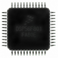
DSP56F801FA80E Freescale Semiconductor, DSP56F801FA80E Datasheet - Page 4

DSP56F801FA80E
Manufacturer Part Number
DSP56F801FA80E
Description
IC DSP 80MHZ 8K FLASH 48-LQFP
Manufacturer
Freescale Semiconductor
Series
56F8xxr
Datasheet
1.DSP56F801EVM.pdf
(48 pages)
Specifications of DSP56F801FA80E
Core Processor
56800
Core Size
16-Bit
Speed
80MHz
Connectivity
SCI, SPI
Peripherals
POR, PWM, WDT
Number Of I /o
11
Program Memory Size
20KB (10K x 16)
Program Memory Type
FLASH
Ram Size
2K x 16
Voltage - Supply (vcc/vdd)
3 V ~ 3.6 V
Data Converters
A/D 8x12b
Oscillator Type
Internal
Operating Temperature
-40°C ~ 85°C
Package / Case
48-LQFP
Package
48LQFP
Family Name
56F8xx
Maximum Speed
80 MHz
Operating Supply Voltage
3.3 V
Data Bus Width
16 Bit
Number Of Programmable I/os
11
Interface Type
SCI/SPI
On-chip Adc
2(4-chx12-bit)
Number Of Timers
1
Lead Free Status / RoHS Status
Lead free / RoHS Compliant
Eeprom Size
-
Available stocks
Company
Part Number
Manufacturer
Quantity
Price
Company:
Part Number:
DSP56F801FA80E
Manufacturer:
Freescale Semiconductor
Quantity:
10 000
Part Number:
DSP56F801FA80E
Manufacturer:
FREESCALE
Quantity:
20 000
Part 1 Overview
1.1 56F801 Features
1.1.1
1.1.2
1.1.3
4
•
•
•
•
•
•
•
•
•
•
•
•
•
•
•
•
•
•
•
•
•
•
Efficient 16-bit 56800 family controller engine with dual Harvard architecture
As many as 40 Million Instructions Per Second (MIPS) at 80MHz core frequency
Single-cycle 16 × 16-bit parallel Multiplier-Accumulator (MAC)
Two 36-bit accumulators including extension bits
16-bit bidirectional barrel shifter
Parallel instruction set with unique processor addressing modes
Hardware DO and REP loops
Three internal address buses and one external address bus
Four internal data buses and one external data bus
Instruction set supports both DSP and controller functions
Controller style addressing modes and instructions for compact code
Efficient C compiler and local variable support
Software subroutine and interrupt stack with depth limited only by memory
JTAG/OnCE debug programming interface
Harvard architecture permits as many as three simultaneous accesses to Program and Data memory
On-chip memory including a low-cost, high-volume Flash solution
— 8K × 16 bit words of Program Flash
— 1K × 16-bit words of Program RAM
— 2K × 16-bit words of Data Flash
— 1K × 16-bit words of Data RAM
— 2K × 16-bit words of Boot Flash
Programmable Boot Flash supports customized boot code and field upgrades of stored code through a
variety of interfaces (JTAG, SPI)
Pulse Width Modulator (PWM) with six PWM outputs, two Fault inputs, fault-tolerant design with deadtime
insertion; supports both center- and edge-aligned modes
Two 12-bit, Analog-to-Digital Converters (ADCs), which support two simultaneous conversions with two
4-multiplexed inputs; ADC and PWM modules can be synchronized
General Purpose Quad Timer: Timer D with three pins (or three additional GPIO lines)
Serial Communication Interface (SCI) with two pins (or two additional GPIO lines)
Serial Peripheral Interface (SPI) with configurable four-pin port (or four additional GPIO lines)
Digital Signal Processing Core
Memory
Peripheral Circuits for 56F801
56F801 Technical Data, Rev. 17
Freescale Semiconductor


