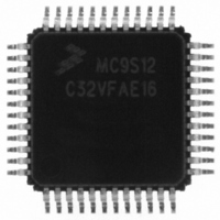
MC9S12C32VFAE16 Freescale Semiconductor, MC9S12C32VFAE16 Datasheet - Page 195

MC9S12C32VFAE16
Manufacturer Part Number
MC9S12C32VFAE16
Description
IC MCU 32K FLASH 16MHZ 48-LQFP
Manufacturer
Freescale Semiconductor
Series
HCS12r
Datasheets
1.MC9S12GC16MFUE.pdf
(690 pages)
2.MC9S12C96CFUER.pdf
(26 pages)
3.MC9S12C32CFAE25.pdf
(2 pages)
Specifications of MC9S12C32VFAE16
Core Processor
HCS12
Core Size
16-Bit
Speed
16MHz
Connectivity
CAN, EBI/EMI, SCI, SPI
Peripherals
POR, PWM, WDT
Number Of I /o
31
Program Memory Size
32KB (32K x 8)
Program Memory Type
FLASH
Ram Size
2K x 8
Voltage - Supply (vcc/vdd)
2.35 V ~ 5.5 V
Data Converters
A/D 8x10b
Oscillator Type
Internal
Operating Temperature
-40°C ~ 105°C
Package / Case
48-LQFP
For Use With
CML12C32SLK - KIT STUDENT LEARNING 16BIT HCS12
Lead Free Status / RoHS Status
Lead free / RoHS Compliant
Eeprom Size
-
Available stocks
Company
Part Number
Manufacturer
Quantity
Price
Company:
Part Number:
MC9S12C32VFAE16
Manufacturer:
Freescale Semiconductor
Quantity:
10 000
- Current page: 195 of 690
- Download datasheet (4Mb)
7.2
The DBG sub-module relies on the external bus interface (generally the MEBI) when the DBG is matching
on the external bus.
The tag pins in
Freescale Semiconductor
PE3/LSTRB/ TAGLO
BKGD/MODC/
CPU PROGRAM COUNTER
INSTRUCTION
Pin Name
LAST CYCLE
BUS CLOCK
TAGHI
External Signal Description
WRITE DATA BUS
READ DATA BUS
ADDRESS BUS
WRITE DATA BUS
READ DATA BUS
READ/WRITE
DBG MODE ENABLE
CHANGE-OF-FLOW
INDICATORS
MCU IN BDM
DBG READ DATA BUS
Table 7-1
READ/WRITE
REGISTER
Pin Functions
Table 7-1. External System Pins Associated with DBG and MEBI
TAGLO
TAGHI
(part of the MEBI) may also be a part of the breakpoint operation.
Figure 7-2. DBG Block Diagram in DBG Mode
M
U
X
When instruction tagging is on, a 0 at the falling edge of E tags the high half of the
instruction word being read into the instruction queue.
In expanded wide mode or emulation narrow modes, when instruction tagging is on
and low strobe is enabled, a 0 at the falling edge of E tags the low half of the
instruction word being read into the instruction queue.
MC9S12C-Family / MC9S12GC-Family
M
U
X
INSTRUCTION
ADDRESS/DATA/CONTROL
ADDRESS
M
U
X
COMPARATOR A
COMPARATOR B
COMPARATOR C
LAST
REGISTERS
Rev 01.24
64 x 16 BIT
REGISTER
CAPTURE
PROFILE
BUFFER
TRACE
WORD
Chapter 7 Debug Module (DBGV1) Block Description
Description
CONTROL
MATCH_A
MATCH_B
MATCH_C
LOOP1
EVENT ONLY
POINTER
M
U
X
STORE
DETAIL
PROFILE CAPTURE MODE
CONTROL
TRACER
OR PROFILING DATA
BUFFER
LOGIC
TRACE BUFFER
TAG
FORCE
195
Related parts for MC9S12C32VFAE16
Image
Part Number
Description
Manufacturer
Datasheet
Request
R
Part Number:
Description:
Manufacturer:
Freescale Semiconductor, Inc
Datasheet:
Part Number:
Description:
Manufacturer:
Freescale Semiconductor, Inc
Datasheet:
Part Number:
Description:
Manufacturer:
Freescale Semiconductor, Inc
Datasheet:
Part Number:
Description:
Manufacturer:
Freescale Semiconductor, Inc
Datasheet:
Part Number:
Description:
Manufacturer:
Freescale Semiconductor, Inc
Datasheet:
Part Number:
Description:
Manufacturer:
Freescale Semiconductor, Inc
Datasheet:
Part Number:
Description:
Manufacturer:
Freescale Semiconductor, Inc
Datasheet:
Part Number:
Description:
Manufacturer:
Freescale Semiconductor, Inc
Datasheet:
Part Number:
Description:
Manufacturer:
Freescale Semiconductor, Inc
Datasheet:
Part Number:
Description:
Manufacturer:
Freescale Semiconductor, Inc
Datasheet:
Part Number:
Description:
Manufacturer:
Freescale Semiconductor, Inc
Datasheet:
Part Number:
Description:
Manufacturer:
Freescale Semiconductor, Inc
Datasheet:
Part Number:
Description:
Manufacturer:
Freescale Semiconductor, Inc
Datasheet:
Part Number:
Description:
Manufacturer:
Freescale Semiconductor, Inc
Datasheet:
Part Number:
Description:
Manufacturer:
Freescale Semiconductor, Inc
Datasheet:


