M30622SAFP#U5 Renesas Electronics America, M30622SAFP#U5 Datasheet - Page 273
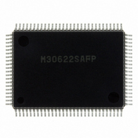
M30622SAFP#U5
Manufacturer Part Number
M30622SAFP#U5
Description
IC M16C MPU ROMLESS 100QFP
Manufacturer
Renesas Electronics America
Series
M16C™ M16C/60r
Datasheets
1.QSK-62P_PLUS.pdf
(103 pages)
2.M30622SAFPU5.pdf
(277 pages)
3.M30622SAFPU5.pdf
(617 pages)
4.M30622SAFPU5.pdf
(308 pages)
Specifications of M30622SAFP#U5
Core Processor
M16C/60
Core Size
16-Bit
Speed
16MHz
Connectivity
SIO, UART/USART
Peripherals
DMA, PWM, WDT
Number Of I /o
50
Program Memory Type
ROMless
Ram Size
3K x 8
Voltage - Supply (vcc/vdd)
4.2 V ~ 5.5 V
Data Converters
A/D 10x10b, D/A 2x8b
Oscillator Type
Internal
Operating Temperature
-20°C ~ 85°C
Package / Case
100-QFP
For Use With
867-1000 - KIT QUICK START RENESAS 62PM3062PT3-CPE-3 - EMULATOR COMPACT M16C/62P/30P
Lead Free Status / RoHS Status
Lead free / RoHS Compliant
Eeprom Size
-
Program Memory Size
-
Available stocks
Company
Part Number
Manufacturer
Quantity
Price


270
Revision History
REV.A1
REV. A2
Version
REV. B
Revision history
Page 145 Note 2
Page 115, 139, Bit 3 of the UART2 special mode register 2 (bit symbol)
Page 43, Figure 1.10.6
Page 144, Figure 1.16.32, bit 5 of the SI/Oi control register (i=3, 4)
Page 144, Figure 1.16.32, Note 2
Page 2 Note is added in Figure 1.1.1.
Page 3 Note is added in Figure 1.1.2.
Page 10 Explanation of “Memory” is partly revised.
Page 10 Figure 1.3.1 is partly revised.
Page 22 Figure 1.7.1 is partly revised.
Page 23 Figure 1.7.2 is partly revised.
Page 23 “Internal Reserved Area Expansion Bit (PM13)” is added.
Page 24 Figure 1.7.3 is partly revised.
Page 25 Explanation of “(3) Selecting separate/multiplex bus” is partly revised.
Page 28 Explanation of “(2) Chip select signal” is partly added.
Page 29 Figure 1.9.2 is added.
Page 37 Explanation of “(2) Sub-clock” is partly revised.
Page 38 Figure 1.10.4 is partly revised.
Page 39 Explanation of “Stop Mode” is partly revised.
Page 39 Table 1.10.2 is partly revised.
Page 40 Explanation of “Wait Mode” is partly revised.
Page 40 Table 1.10.3 is partly revised.
Page 42 Explanation of “Power Control” is partly revised.
Page 62 Explanation of “Address Match Interruptl” is partly revised.
• Before data can be written to the SI/Oi transmit/receive register (addresses
0360
the SI/Oi Control Register (addresses 0362
set bit), make sure the CLKi pin input is held low. ---> • Before data can be written
to the SI/Oi transmit/receive register (addresses 0360
input must be in the high state. Also, before rewriting the SI/Oi Control Register
(addresses 0362
pin input is held high.
ASL --> ALS
Note: Writing a value to an address after “1” is written to this bit returns the bit to
Transfer direction lect bit --->Transfer direction select bit
When using the port as an input/output port by setting the SI/Oi port select bit (i =
3, 4) to “1”, be sure to set the sync clock select bit to “1”.
--->
When using the port as an input/output port by setting the SI/Oi port select bit (i =
3, 4) to “0”, be sure to set the sync clock select bit to “1”.
16
“0” . Other bits do not automatically return to “0” and they must therefore
be reset by the program.
, 0364
16
), the CLKi pin input must be in the low state. Also, before rewriting
16
, 0366
16
M16C/62A Group data sheet
)’s bit 7 (S
Contents for change
OUTi
initial value set bit), make sure the CLKi
16
, 0366
16
)’s bit 7 (S
16
, 0364
SINGLE-CHIP 16-BIT CMOS MICROCOMPUTER
16
OUTi
), the CLKi pin
initial value
M16C / 62A Group
Mitsubishi microcomputers
Revision
01.3.27
99.12.21
00.7.10
00.7.3
date
Related parts for M30622SAFP#U5
Image
Part Number
Description
Manufacturer
Datasheet
Request
R

Part Number:
Description:
KIT STARTER FOR M16C/29
Manufacturer:
Renesas Electronics America
Datasheet:

Part Number:
Description:
KIT STARTER FOR R8C/2D
Manufacturer:
Renesas Electronics America
Datasheet:

Part Number:
Description:
R0K33062P STARTER KIT
Manufacturer:
Renesas Electronics America
Datasheet:

Part Number:
Description:
KIT STARTER FOR R8C/23 E8A
Manufacturer:
Renesas Electronics America
Datasheet:

Part Number:
Description:
KIT STARTER FOR R8C/25
Manufacturer:
Renesas Electronics America
Datasheet:

Part Number:
Description:
KIT STARTER H8S2456 SHARPE DSPLY
Manufacturer:
Renesas Electronics America
Datasheet:

Part Number:
Description:
KIT STARTER FOR R8C38C
Manufacturer:
Renesas Electronics America
Datasheet:

Part Number:
Description:
KIT STARTER FOR R8C35C
Manufacturer:
Renesas Electronics America
Datasheet:

Part Number:
Description:
KIT STARTER FOR R8CL3AC+LCD APPS
Manufacturer:
Renesas Electronics America
Datasheet:
Part Number:
Description:
KIT STARTER FOR RX610
Manufacturer:
Renesas Electronics America
Datasheet:

Part Number:
Description:
KIT STARTER FOR R32C/118
Manufacturer:
Renesas Electronics America
Datasheet:

Part Number:
Description:
KIT DEV RSK-R8C/26-29
Manufacturer:
Renesas Electronics America
Datasheet:

Part Number:
Description:
KIT STARTER FOR SH7124
Manufacturer:
Renesas Electronics America
Datasheet:

Part Number:
Description:
KIT STARTER FOR H8SX/1622
Manufacturer:
Renesas Electronics America
Datasheet:

Part Number:
Description:
KIT DEV FOR SH7203
Manufacturer:
Renesas Electronics America
Datasheet: