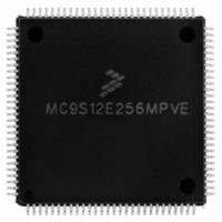
MC9S12E256MPVE Freescale Semiconductor, MC9S12E256MPVE Datasheet - Page 582

MC9S12E256MPVE
Manufacturer Part Number
MC9S12E256MPVE
Description
IC MCU 256K FLASH 25MHZ 112-LQFP
Manufacturer
Freescale Semiconductor
Series
HCS12r
Specifications of MC9S12E256MPVE
Core Processor
HCS12
Core Size
16-Bit
Speed
25MHz
Connectivity
EBI/EMI, I²C, SCI, SPI
Peripherals
POR, PWM, WDT
Number Of I /o
91
Program Memory Size
256KB (256K x 8)
Program Memory Type
FLASH
Ram Size
16K x 8
Voltage - Supply (vcc/vdd)
2.35 V ~ 2.75 V
Data Converters
A/D 16x10b; D/A 2x8b
Oscillator Type
Internal
Operating Temperature
-40°C ~ 125°C
Package / Case
112-LQFP
Processor Series
S12E
Core
HCS12
Data Bus Width
16 bit
Data Ram Size
16 KB
Interface Type
I2C/SCI/SPI
Maximum Clock Frequency
50 MHz
Number Of Programmable I/os
92
Number Of Timers
12
Operating Supply Voltage
0 V to 5 V
Maximum Operating Temperature
+ 125 C
Mounting Style
SMD/SMT
3rd Party Development Tools
EWHCS12
Minimum Operating Temperature
- 40 C
On-chip Adc
16-ch x 10-bit
On-chip Dac
2-ch x 8-bit
For Use With
M68EVB912E128 - BOARD EVAL FOR MC9S12E128/64
Lead Free Status / RoHS Status
Lead free / RoHS Compliant
Eeprom Size
-
Lead Free Status / Rohs Status
Lead free / RoHS Compliant
Available stocks
Company
Part Number
Manufacturer
Quantity
Price
Company:
Part Number:
MC9S12E256MPVE
Manufacturer:
Freescale Semiconductor
Quantity:
10 000
- Current page: 582 of 602
- Download datasheet (4Mb)
Appendix A Electrical Characteristics
In
In
582
Num
Figure A-6
Table A-17
10
11
12
13
(CPOL = 0)
(CPOL = 1)
1
1
2
3
4
5
6
9
(OUTPUT)
(OUTPUT)
(OUTPUT)
(OUTPUT)
1.If configured as output
2. LSBF = 0. For LSBF = 1, bit order is LSB, bit 1, ..., bit 6, MSB.
(INPUT)
MISO
MOSI
SCK
SCK
SS
C
P
P
D
D
D
D
D
D
D
D
D
D
1
PORT DATA
the timing diagram for master mode with transmission format CPHA=1 is depicted.
the timing characteristics for master mode are listed.
SCK Frequency
SCK Period
Enable Lead Time
Enable Lag Time
Clock (SCK) High or Low Time
Data Setup Time (Inputs)
Data Hold Time (Inputs)
Data Valid after SCK Edge
Data Valid after SS fall (CPHA = 0)
Data Hold Time (Outputs)
Rise and Fall Time Inputs
Rise and Fall Time Outputs
9
2
4
MASTER MSB OUT
Table A-17. SPI Master Mode Timing Characteristics
5
Characteristic
MSB IN
1
Figure A-6. SPI Master Timing (CPHA=1)
2
6
4
MC9S12E256 Data Sheet, Rev. 1.08
2
12
12
11
BIT 6 . . . 1
BIT 6 . . . 1
Symbol
t
t
t
f
wsck
t
t
t
lead
vsck
t
t
t
t
sck
sck
t
vss
lag
su
ho
rfo
hi
rfi
13
13
MASTER LSB OUT
1/2048
Min
20
—
—
—
—
—
—
—
2
8
8
LSB IN
Typ
1/2
1/2
1/2
—
—
—
—
—
—
—
—
—
3
Freescale Semiconductor
PORT DATA
2048
Max
1 2
30
15
—
—
—
—
—
—
8
8
Unit
f
t
t
t
t
bus
bus
ns
ns
ns
ns
ns
ns
ns
sck
sck
sck
Related parts for MC9S12E256MPVE
Image
Part Number
Description
Manufacturer
Datasheet
Request
R
Part Number:
Description:
Manufacturer:
Freescale Semiconductor, Inc
Datasheet:
Part Number:
Description:
Manufacturer:
Freescale Semiconductor, Inc
Datasheet:
Part Number:
Description:
Manufacturer:
Freescale Semiconductor, Inc
Datasheet:
Part Number:
Description:
Manufacturer:
Freescale Semiconductor, Inc
Datasheet:
Part Number:
Description:
Manufacturer:
Freescale Semiconductor, Inc
Datasheet:
Part Number:
Description:
Manufacturer:
Freescale Semiconductor, Inc
Datasheet:
Part Number:
Description:
Manufacturer:
Freescale Semiconductor, Inc
Datasheet:
Part Number:
Description:
Manufacturer:
Freescale Semiconductor, Inc
Datasheet:
Part Number:
Description:
Manufacturer:
Freescale Semiconductor, Inc
Datasheet:
Part Number:
Description:
Manufacturer:
Freescale Semiconductor, Inc
Datasheet:
Part Number:
Description:
Manufacturer:
Freescale Semiconductor, Inc
Datasheet:
Part Number:
Description:
Manufacturer:
Freescale Semiconductor, Inc
Datasheet:
Part Number:
Description:
Manufacturer:
Freescale Semiconductor, Inc
Datasheet:
Part Number:
Description:
Manufacturer:
Freescale Semiconductor, Inc
Datasheet:
Part Number:
Description:
Manufacturer:
Freescale Semiconductor, Inc
Datasheet:


