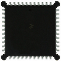
MC68332GCEH16 Freescale Semiconductor, MC68332GCEH16 Datasheet - Page 57

MC68332GCEH16
Manufacturer Part Number
MC68332GCEH16
Description
IC MCU 32BIT 16MHZ 132-PQFP
Manufacturer
Freescale Semiconductor
Series
M683xxr
Specifications of MC68332GCEH16
Core Processor
CPU32
Core Size
32-Bit
Speed
16MHz
Connectivity
EBI/EMI, SCI, SPI, UART/USART
Peripherals
POR, PWM, WDT
Number Of I /o
15
Program Memory Type
ROMless
Ram Size
2K x 8
Voltage - Supply (vcc/vdd)
4.5 V ~ 5.5 V
Oscillator Type
Internal
Operating Temperature
-40°C ~ 85°C
Package / Case
132-QFP
Cpu Family
68K/M683xx
Device Core
ColdFire
Device Core Size
32b
Frequency (max)
16MHz
Interface Type
QSPI/SCI/UART
Program Memory Size
Not Required
Total Internal Ram Size
2KB
# I/os (max)
15
Number Of Timers - General Purpose
16
Operating Supply Voltage (typ)
5V
Operating Supply Voltage (max)
5.5V
Operating Supply Voltage (min)
4.5V
Instruction Set Architecture
RISC
Operating Temp Range
-40C to 85C
Operating Temperature Classification
Industrial
Mounting
Surface Mount
Pin Count
132
Package Type
PQFP
Controller Family/series
68K
No. Of I/o's
15
Ram Memory Size
2KB
Cpu Speed
16MHz
No. Of Timers
16
Embedded Interface Type
QSPI, SCI, UART
Digital Ic Case Style
PQFP
Rohs Compliant
Yes
Processor Series
M683xx
Core
CPU32
Data Bus Width
32 bit
Data Ram Size
2 KB
Maximum Clock Frequency
16 MHz
Number Of Programmable I/os
15
Number Of Timers
16
Maximum Operating Temperature
+ 85 C
Mounting Style
SMD/SMT
Minimum Operating Temperature
- 40 C
Lead Free Status / RoHS Status
Lead free / RoHS Compliant
Eeprom Size
-
Program Memory Size
-
Data Converters
-
Lead Free Status / Rohs Status
Compliant
Available stocks
Company
Part Number
Manufacturer
Quantity
Price
Company:
Part Number:
MC68332GCEH16
Manufacturer:
Freescale Semiconductor
Quantity:
10 000
5.2.9 Frequency Measurement (FQM)
5.2.10 Hall Effect Decode (HALLD)
5.3 Programmer's Model
MC68332
MC68332TS/D
FQM counts the number of input pulses to a TPU channel during a user-defined window period. The
function has single shot and continuous modes. No pulses are lost between sample windows in contin-
uous mode. The user selects whether to detect pulses on the rising or falling edge. This function is in-
tended for high speed measurement; measurement of slow pulses with noise rejection can be made
with PTA.
This function decodes the sensor signals from a brushless motor, along with a direction input from the
CPU, into a state number. The function supports two- or three-sensor decoding. The decoded state
number is written into a COMM channel, which outputs the required commutation drive signals. In ad-
dition to brushless motor applications, the function can have more general applications, such as decod-
ing “option” switches.
The TPU control register address map occupies 512 bytes. The “Access” column in the TPU address
map below indicates which registers are accessible only at the supervisor privilege level and which can
be assigned to either the supervisor or user privilege level, according to the value of the SUPV bit in the
TPUMCR.
Y = M111, where M represents the logic state of the module mapping (MM) bit in the SIMCR.
Access
S/U
S/U
S/U
S/U
S
S
S
S
S
S
S
S
S
S
S
S
S
S
S
S
$YFFE0C
$YFFE1C
$YFFE00
$YFFE02
$YFFE04
$YFFE06
$YFFE08
$YFFE0A
$YFFE0E
$YFFE10
$YFFE12
$YFFE14
$YFFE16
$YFFE18
$YFFE1A
$YFFE1E
$YFFE20
$YFFE22
$YFFE24
$YFFE26
Address
Freescale Semiconductor, Inc.
For More Information On This Product,
15
Table 22 TPU Address Map
Go to: www.freescale.com
DEVELOPMENT SUPPORT CONTROL REGISTER (DSCR)
CHANNEL FUNCTION SELECTION REGISTER 0 (CFSR0)
CHANNEL FUNCTION SELECTION REGISTER 1 (CFSR1)
CHANNEL FUNCTION SELECTION REGISTER 2 (CFSR2)
CHANNEL FUNCTION SELECTION REGISTER 3 (CFSR3)
DEVELOPMENT SUPPORT STATUS REGISTER (DSSR)
TPU MODULE CONFIGURATION REGISTER (TPUMCR)
TPU INTERRUPT CONFIGURATION REGISTER (TICR)
DECODED CHANNEL NUMBER REGISTER (DCNR)
CHANNEL INTERRUPT ENABLE REGISTER (CIER)
CHANNEL INTERRUPT STATUS REGISTER (CISR)
HOST SERVICE REQUEST REGISTER 0 (HSRR0)
HOST SERVICE REQUEST REGISTER 1 (HSRR1)
SERVICE GRANT LATCH REGISTER (SGLR)
TEST CONFIGURATION REGISTER (TCR)
CHANNEL PRIORITY REGISTER 0 (CPR0)
CHANNEL PRIORITY REGISTER 1 (CPR1)
HOST SEQUENCE REGISTER 0 (HSQR0)
HOST SEQUENCE REGISTER 1 (HSQR1)
LINK REGISTER (LR)
8
7
MOTOROLA
0
57


