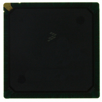
MCF5474VR266 Freescale Semiconductor, MCF5474VR266 Datasheet - Page 21

MCF5474VR266
Manufacturer Part Number
MCF5474VR266
Description
IC MPU 32BIT COLDF 388-PBGA
Manufacturer
Freescale Semiconductor
Series
MCF547xr
Datasheet
1.MCF5472VR200.pdf
(34 pages)
Specifications of MCF5474VR266
Core Processor
Coldfire V4E
Core Size
32-Bit
Speed
266MHz
Connectivity
EBI/EMI, Ethernet, I²C, SPI, UART/USART, USB
Peripherals
DMA, PWM, WDT
Number Of I /o
99
Program Memory Type
ROMless
Ram Size
32K x 8
Voltage - Supply (vcc/vdd)
1.43 V ~ 1.58 V
Oscillator Type
External
Operating Temperature
0°C ~ 70°C
Package / Case
388-BGA
Family Name
MCF5xxx
Device Core
ColdFire V4e
Device Core Size
32b
Frequency (max)
266MHz
Instruction Set Architecture
RISC
Supply Voltage 1 (typ)
1.5/3.3V
Operating Supply Voltage (max)
1.58/3.6V
Operating Supply Voltage (min)
1.43/3V
Operating Temp Range
0C to 70C
Operating Temperature Classification
Commercial
Mounting
Surface Mount
Pin Count
388
Package Type
BGA
Processor Series
MCF547x
Core
ColdFire V4
Data Bus Width
32 bit
Program Memory Size
32 KB
Data Ram Size
32 KB
Interface Type
I2C, JTAG
Maximum Clock Frequency
83 MHz
Operating Supply Voltage
3 V to 3.6 V
Maximum Operating Temperature
+ 70 C
Mounting Style
SMD/SMT
3rd Party Development Tools
JLINK-CF-BDM26, EWCF
Development Tools By Supplier
M5475EVBE
Minimum Operating Temperature
0 C
Cpu Speed
266MHz
Embedded Interface Type
I2C, UART, DMA
Digital Ic Case Style
BGA
No. Of Pins
388
Rohs Compliant
Yes
For Use With
M5475EVBGHS - KIT DEV GHS FOR M5475EVBM5474GFE - MODULE M5474 FIRE ENGINEM5474LITEKIT - KIT DEV FOR MCF547X
Lead Free Status / RoHS Status
Lead free / RoHS Compliant
Eeprom Size
-
Program Memory Size
-
Data Converters
-
Lead Free Status / Rohs Status
Compliant
Available stocks
Company
Part Number
Manufacturer
Quantity
Price
Company:
Part Number:
MCF5474VR266
Manufacturer:
Freescale Semiconductor
Quantity:
135
Company:
Part Number:
MCF5474VR266
Manufacturer:
Freescale Semiconductor
Quantity:
10 000
10
The PCI bus on the MCF54
refer to the PCI 2.2 spec for a more detailed timing analysis.
Freescale Semiconductor
Num
SDCSn,SDWE,
P1
P2
P3
P4
P5
P6
PCI Bus
SDBA[1:0]
RAS, CAS
SDADDR,
SDCLK0
SDCLK1
SDCLK0
SDCLK1
Frequency of Operation
Clock Period (t
Address, Data, and Command (33< PCI ≤ 66 Mhz)—Input Setup (t
Address, Data, and Command (0 < PCI ≤ 33 Mhz)—Input Setup (t
Address, Data, and Command (33–66 Mhz)—Output Valid (t
Address, Data, and Command (0–33 Mhz) - Output Valid (t
PCI signals (0–66 Mhz) - Output Hold (t
SDDATA
SDDATA
SDDQS
SDDQS
7
x is PCI 2.2 compliant. The following timing numbers are mostly from the PCI 2.2 spec. Please
CK
DD4
)
ROW
CMD
MCF547x ColdFire
Table 14. PCI Timing Specifications
Characteristic
DD1
Figure 17. DDR Read Timing
DD5
DH
)
®
COL
Microprocessor, Rev. 4
CL=2
CL=2.5
DV
DD2
DQS Read
DD10
DV
Preamble
)
)
DQS Read
DD3
Preamble
IS
IS
)
)
WD1 WD2 WD3 WD4
15.15
Min
3.0
7.0
25
—
—
0
WD1 WD2 WD3 WD4
DD9
Max
11.0
6.0
66
40
—
—
—
DQS Read
Postamble
MHz
Unit
ns
ns
ns
ns
ns
ns
DQS Read
Postamble
Notes
1
2
3
4
PCI Bus
21


