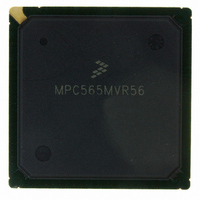
MPC565MVR56 Freescale Semiconductor, MPC565MVR56 Datasheet - Page 5

MPC565MVR56
Manufacturer Part Number
MPC565MVR56
Description
IC MCU 1M FLASH 56MHZ 388-BGA
Manufacturer
Freescale Semiconductor
Series
MPC5xxr
Datasheet
1.MPC565CVR40.pdf
(16 pages)
Specifications of MPC565MVR56
Core Processor
PowerPC
Core Size
32-Bit
Speed
56MHz
Connectivity
CAN, EBI/EMI, SCI, SPI, UART/USART
Peripherals
POR, PWM, WDT
Number Of I /o
56
Program Memory Size
1MB (1M x 8)
Program Memory Type
FLASH
Ram Size
36K x 8
Voltage - Supply (vcc/vdd)
2.5 V ~ 2.7 V
Data Converters
A/D 40x10b
Oscillator Type
External
Operating Temperature
-40°C ~ 125°C
Package / Case
388-BGA
Processor Series
MPC5xx
Core
PowerPC
Data Bus Width
32 bit
Data Ram Size
36 KB
Interface Type
QSPI/SCI/UART
Maximum Clock Frequency
56 MHz
Number Of Programmable I/os
56
Number Of Timers
3
Operating Supply Voltage
0 V to 5 V
Maximum Operating Temperature
+ 125 C
Mounting Style
SMD/SMT
Development Tools By Supplier
MPC566EVBE
Minimum Operating Temperature
- 40 C
On-chip Adc
2 (40-ch x 10-bit)
Lead Free Status / RoHS Status
Lead free / RoHS Compliant
Eeprom Size
-
Lead Free Status / Rohs Status
Lead free / RoHS Compliant
Available stocks
Company
Part Number
Manufacturer
Quantity
Price
Company:
Part Number:
MPC565MVR56
Manufacturer:
AOS
Quantity:
40
Company:
Part Number:
MPC565MVR56
Manufacturer:
FREESCAL
Quantity:
206
Company:
Part Number:
MPC565MVR56
Manufacturer:
Freescale Semiconductor
Quantity:
10 000
Company:
Part Number:
MPC565MVR56R2
Manufacturer:
Freescale Semiconductor
Quantity:
10 000
1.2.10 Debug Features
1.2.10.1 Nexus Debug Port (Class 3)
1.2.10.2 Message Data Link Controller (DLCMD2) Module
1.2.11 Integrated I/O System
1.2.11.1 Time Processor Units (TPU3)
MOTOROLA
•
•
•
•
•
•
•
•
•
•
•
•
•
•
•
•
•
•
•
•
•
•
•
•
•
Extensive system debug support
On-chip watchpoints and breakpoints
Program flow tracking
Background debug mode (BDM)
Nexus/IEEE – ISTO 5001-1999 debug port (Class 3)
Nine- or 16-pin interface
Two pins muxed with QSMCMB pins. Muxing controlled by QSMCMB PCS3 pin assignment
register
SAE J1850 Class B data communications network interface compatible and ISO compatible for
low-speed ( < 125 Kbps) serial data communications in automotive applications
10.4 Kbps variable pulse width (VPW) bit format
Digital noise filter, collision detection
Hardware cyclical redundancy check (CRC) generation and checking
Block mode receive and transmit supported
4x receive mode supported (41.6 Kbps)
Digital loopback mode
In-frame response (IFR) types 0, 1, 2, and 3 supported
Dedicated register for symbol timing adjustments
Inter-module bus 3 (IMB3) slave interface
Power-saving IMB3 stop mode with automatic wakeup on network activity
Power-saving IMB3 CLOCKDIS mode
Debug mode available through IMB3 FREEZE signal or user controllable SOFT_FRZ bit
Polling and IMB3 interrupt generation with vector lookup available
True 5-V I/O
Three time processing units (TPU3)
— 16 channels each
Each TPU3 is a microcoded timer subsystem
One 6-Kbyte and one 4-Kbyte dual-port TPU RAM (DPTRAM), one (6-Kbyte) shared by two
TPU3 modules for TPU microcode and the 4-Kbyte dedicated to the third TPU3 for microcode.
Freescale Semiconductor, Inc.
For More Information On This Product,
MPC565/MPC566 Product Brief
Go to: www.freescale.com
Detailed Feature List
5


