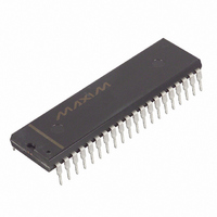
DS80C310-MCG+ Maxim Integrated Products, DS80C310-MCG+ Datasheet - Page 12

DS80C310-MCG+
Manufacturer Part Number
DS80C310-MCG+
Description
IC MCU HI SPEED 25MHZ 40-DIP
Manufacturer
Maxim Integrated Products
Series
80Cr
Datasheet
1.DS80C310FCG.pdf
(22 pages)
Specifications of DS80C310-MCG+
Core Processor
8051
Core Size
8-Bit
Speed
25MHz
Connectivity
EBI/EMI, SIO, UART/USART
Peripherals
Brown-out Detect/Reset, POR
Number Of I /o
32
Program Memory Type
ROMless
Ram Size
256 x 8
Voltage - Supply (vcc/vdd)
4.5 V ~ 5.5 V
Oscillator Type
External
Operating Temperature
0°C ~ 70°C
Package / Case
40-DIP (0.600", 15.24mm)
Processor Series
80C
Core
8051
Data Bus Width
8 bit
Program Memory Size
64 KB
Data Ram Size
64 KB
Maximum Clock Frequency
25 MHz
Number Of Programmable I/os
32
Number Of Timers
3
Operating Supply Voltage
5 V
Maximum Operating Temperature
+ 70 C
Mounting Style
Through Hole
3rd Party Development Tools
PK51, CA51, A51, ULINK2
Minimum Operating Temperature
0 C
Controller Family/series
(8051) 8052
No. Of I/o's
32
Ram Memory Size
256Byte
Cpu Speed
25MHz
No. Of Timers
3
Embedded Interface Type
UART
Digital Ic Case Style
DIP
Rohs Compliant
Yes
Interface Type
UART
Lead Free Status / RoHS Status
Lead free / RoHS Compliant
Eeprom Size
-
Program Memory Size
-
Data Converters
-
Lead Free Status / Rohs Status
Lead free / RoHS Compliant
Figure 2. Typical I
Note 6:
Note 7:
Note 8:
Note 9:
Note 10:
Note 11:
cycles following 1 to 0 transitions, the typical current sink capability of Port 0 and Port 2 is approximately 150A, and the
minimum current sink capability of ALE and PSEN is approximately 400A. On subsequent cycles following 0 to 1
transitions, the typical current drive capability of Port 0 and Port 2 is approximately 110A.
mode.
This is only the current required to hold the low level; transitions from 1 to 0 on an I/O pin must also overcome the transition
current.
2V.
address bus on the DS80C310. Peak current occurs near the input transition point of the latch, approximately 2V.
When addressing external memory. This specification applies to the first clock cycle following the transition. On subsequent
RST = V
During a 0 to 1 transition, a one-shot drives the ports hard for two clock cycles. This measurement reflects port in transition
Current required from external circuit to hold a logic-low level on an I/O pin while the corresponding port latch bit is set to 1.
Ports 1 and 3 source transition current when being pulled down externally. The current reaches its maximum at approximately
0.45 < V
IN
CC
<V
. This condition mimics operation of pins in I/O mode.
CC
CC
. Not a high-impedance input. This port is a weak address holding latch because Port 0 is dedicated as an
vs. Frequency
12 of 22
DS80C310


