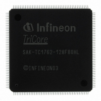
SAK-TC1762-128F80HL AC Infineon Technologies, SAK-TC1762-128F80HL AC Datasheet - Page 34

SAK-TC1762-128F80HL AC
Manufacturer Part Number
SAK-TC1762-128F80HL AC
Description
IC MCU 32BIT FLASH PG-LQFP-176
Manufacturer
Infineon Technologies
Series
TC17xxr
Datasheet
1.SAK-TC1762-128F80HL_AC.pdf
(114 pages)
Specifications of SAK-TC1762-128F80HL AC
Core Processor
TriCore
Core Size
32-Bit
Speed
80MHz
Connectivity
ASC, CAN, MLI, MSC, SSC
Peripherals
DMA, POR, WDT
Number Of I /o
81
Program Memory Size
1MB (1M x 8)
Program Memory Type
FLASH
Ram Size
52K x 8
Voltage - Supply (vcc/vdd)
1.42 V ~ 1.58 V
Data Converters
A/D 2x10b; A/D 32x8b,10b,12b
Oscillator Type
External
Operating Temperature
-40°C ~ 125°C
Package / Case
176-LFQFP
Packages
PG-LQFP-176
Max Clock Frequency
80.0 MHz
Sram (incl. Cache)
52.0 KByte
Can Nodes
2
A / D Input Lines (incl. Fadc)
36
Program Memory
1.0 MB
For Use With
B158-H8539-G2-X-7600IN - KIT STARTER TC176X SERIES
Lead Free Status / RoHS Status
Lead free / RoHS Compliant
Eeprom Size
-
Other names
KT1762128F80HLACXT
SAK-TC1762-128F80HLACINTR
SP000318061
SAK-TC1762-128F80HLACINTR
SP000318061
Preliminary
•
•
•
•
•
•
•
•
•
•
Memory Checker
The Memory Checker Module (MCHK) makes it possible to check the data consistency
of memories. Any SPB bus master may access the memory checker. It is preferable the
DMA does it as described hereafter. It uses DMA 8-bit, 16-bit, or 32-bit moves to read
from the selected address area and to write the value read in a memory checker input
register. With each write operation to the memory checker input register, a polynomial
checksum calculation is triggered and the result of the calculation is stored in the
memory checker result register.
The memory checker uses the standard Ethernet polynomial, which is given by:
G
Note: Although the polynomial above is used for generation, the generation algorithm
Data Sheet
32
– 8 DMA channels in the DMA Sub-Block
– Up to 8 selectable request inputs per DMA channel
– 2-level programmable priority of DMA channels within the DMA Sub-Block
– Software and hardware DMA request
– Hardware requests by selected on-chip peripherals and external inputs
Programmable priority of the DMA Sub-Blocks on the bus interfaces
Buffer capability for move actions on the buses (at least 1 move per bus is buffered).
Individually programmable operation modes for each DMA channel
– Single Mode: stops and disables DMA channel after a predefined number of DMA
– Continuous Mode: DMA channel remains enabled after a predefined number of
– Programmable address modification
Full 32-bit addressing capability of each DMA channel
– 4 Gbyte address range
– Support of circular buffer addressing mode
Programmable data width of DMA transfer/transaction: 8-bit, 16-bit, or 32-bit
Micro Link bus interface support
Register set for each DMA channel
– Source and destination address register
– Channel control and status register
– Transfer count register
Flexible interrupt generation (the service request node logic for the MLI channels is
also implemented in the DMA module)
All buses connected to the DMA module must work at the same frequency.
Read/write requests of the System Bus side to the peripherals on DMA Bus are
bridged to the DMA Bus (only the DMA is the master on the DMA bus), allowing easy
access to these peripherals by CPU
= x
transfers
DMA transfers; DMA transaction can be repeated.
differs from the one that is used by the Ethernet protocol.
32
+ x
26
+ x
23
+ x
22
+ x
16
+ x
12
+ x
11
+ x
10
30
+ x
8
+ x
7
+ x
5
+ x
4
+ x
2
+ x +1
Functional Description
V1.0, 2008-04
TC1762


