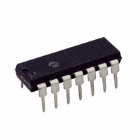
PIC16F526-I/P Microchip Technology, PIC16F526-I/P Datasheet - Page 16

PIC16F526-I/P
Manufacturer Part Number
PIC16F526-I/P
Description
IC PIC MCU FLASH 1KX12 14DIP
Manufacturer
Microchip Technology
Series
PIC® 16Fr
Datasheets
1.PIC16F526-ISL.pdf
(122 pages)
2.PIC16F526-ISL.pdf
(22 pages)
3.PIC16F526-IP.pdf
(104 pages)
Specifications of PIC16F526-I/P
Program Memory Type
FLASH
Program Memory Size
1.5KB (1K x 12)
Package / Case
14-DIP (0.300", 7.62mm)
Core Processor
PIC
Core Size
8-Bit
Speed
20MHz
Peripherals
POR, WDT
Number Of I /o
11
Ram Size
67 x 8
Voltage - Supply (vcc/vdd)
2 V ~ 5.5 V
Data Converters
A/D 3x8b
Oscillator Type
Internal
Operating Temperature
-40°C ~ 85°C
Processor Series
PIC16F
Core
PIC
Data Bus Width
8 bit
Data Ram Size
67 B
Maximum Clock Frequency
20 MHz
Number Of Programmable I/os
12
Number Of Timers
1
Maximum Operating Temperature
+ 85 C
Mounting Style
Through Hole
3rd Party Development Tools
52715-96, 52716-328, 52717-734
Development Tools By Supplier
PG164130, DV164035, DV244005, DV164005, PG164120, ICE2000
Minimum Operating Temperature
- 40 C
On-chip Adc
8 bit, 3 Channel
Lead Free Status / RoHS Status
Lead free / RoHS Compliant
For Use With
AC162096 - HEADER MPLAB ICD2 PIC16F526 8/14
Eeprom Size
-
Connectivity
-
Lead Free Status / Rohs Status
Lead free / RoHS Compliant
PIC16F526
4.2
Data memory is composed of registers or bytes of
SRAM. Therefore, data memory for a device is
specified by its register file. The register file is divided
into two functional groups: Special Function Registers
(SFR) and General Purpose Registers (GPR).
The Special Function Registers are registers used by
the CPU and peripheral functions for controlling
desired operations of the PIC16F526. See Figure 4-1
for details.
The PIC16F526 register file is composed of 16 Special
Function Registers and 67 General Purpose Registers.
FIGURE 4-2:
DS41326E-page 16
Note 1: Not a physical register. See Section 4.8 “Indirect Data Addressing: INDF and FSR Registers”.
Data Memory (SRAM and FSRs)
File Address
FSR<6:5>
0Ch
0Dh
0Ah
0Bh
0Fh
00h
01h
02h
03h
04h
05h
06h
07h
08h
09h
10h
1Fh
REGISTER FILE MAP
CM2CON0
CM1CON0
General
Purpose
Registers
OSCCAL
VRCON
STATUS
ADCON0
PORTB
PORTC
General
Purpose
Registers
INDF
ADRES
TMR0
Bank 0
PCL
FSR
00
(1)
30h
20h
2Fh
3Fh
CM2CON0
CM1CON0
General
Purpose
Registers
PORTC
STATUS
ADCON0
VRCON
EECON
EEDATA
INDF
EEADR
ADRES
FSR
Bank 1
PCL
01
(1)
Addresses map back to
addresses in Bank 0.
50h
40h
4Fh
5Fh
CM1CON0
4.2.1
The General Purpose Register file is accessed, either
directly or indirectly, through the File Select Register
(FSR). See Section 4.8 “Indirect Data Addressing:
INDF and FSR Registers”.
4.2.2
The Special Function Registers (SFRs) are registers
used by the CPU and peripheral functions to control the
operation of the device (Table 4-1).
The Special Function Registers can be classified into
two sets. The Special Function Registers associated
with the “core” functions are described in this section.
Those related to the operation of the peripheral
features are described in the section for each
peripheral feature.
CM2CON0
OSCCAL
VRCON
STATUS
ADCON0
General
Purpose
Registers
PORTB
PORTC
INDF
ADRES
TMR0
FSR
PCL
Bank 2
10
(1)
GENERAL PURPOSE REGISTER
FILE
SPECIAL FUNCTION REGISTERS
70h
60h
6Fh
7Fh
CM1CON0
CM2CON0
STATUS
EEDATA
VRCON
ADCON0
EECON
EEADR
PORTC
INDF
ADRES
General
Purpose
Registers
FSR
Bank 3
PCL
11
(1)
2010 Microchip Technology Inc.


