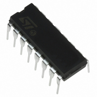
ST7FLITES5Y0B6 STMicroelectronics, ST7FLITES5Y0B6 Datasheet - Page 105

ST7FLITES5Y0B6
Manufacturer Part Number
ST7FLITES5Y0B6
Description
MCU 8BIT 1K FLASH 16DIP
Manufacturer
STMicroelectronics
Series
ST7r
Datasheet
1.ST7FLITES2Y0B6.pdf
(124 pages)
Specifications of ST7FLITES5Y0B6
Core Processor
ST7
Core Size
8-Bit
Speed
8MHz
Connectivity
SPI
Peripherals
LVD, POR, PWM, WDT
Number Of I /o
13
Program Memory Size
1KB (1K x 8)
Program Memory Type
FLASH
Ram Size
128 x 8
Voltage - Supply (vcc/vdd)
2.4 V ~ 5.5 V
Data Converters
A/D 5x10b
Oscillator Type
Internal
Operating Temperature
-40°C ~ 85°C
Package / Case
16-DIP (0.300", 7.62mm)
Processor Series
ST7FLITESx
Core
ST7
Data Bus Width
8 bit
Data Ram Size
128 B
Interface Type
SPI
Maximum Clock Frequency
8 MHz
Number Of Programmable I/os
13
Number Of Timers
2
Operating Supply Voltage
2.4 V to 5.5 V
Maximum Operating Temperature
+ 85 C
Mounting Style
Through Hole
Development Tools By Supplier
ST7FLIT0-IND/USB, ST7FLITE-SK/RAIS, ST7MDT10-DVP3, ST7MDT10-EMU3, STX-RLINK
Minimum Operating Temperature
- 40 C
On-chip Adc
8 bit
For Use With
497-5858 - EVAL BOARD PLAYBACK ST7FLITE497-5049 - KIT STARTER RAISONANCE ST7FLITE
Lead Free Status / RoHS Status
Lead free / RoHS Compliant
Eeprom Size
-
Lead Free Status / Rohs Status
Details
Other names
497-4862
Available stocks
Company
Part Number
Manufacturer
Quantity
Price
ADC CHARACTERISTICS (Cont’d)
Figure 82. R
Notes:
1. C
pacitance (3pF). A high C
2. This graph shows that depending on the input signal variation (f
the use of a larger serial resistor (R
13.11.1 General PCB Design Guidelines
To obtain best results, some general design and
layout rules should be followed when designing
the application PCB to shield the noise-sensitive,
analog physical interface from noise-generating
CMOS logic signals.
Properly place components and route the signal
traces on the PCB to shield the analog inputs. An-
45
40
35
30
25
20
15
10
PARASITIC
5
0
0
represents the capacitance of the PCB (dependent on soldering and PCB layout quality) plus the pad ca-
AIN
max. vs f
10
C
PARASITIC
PARASITIC
(pF)
ADC
30
AIN)
with C
value will downgrade conversion accuracy. To remedy this, f
4 MHz
2 MHz
1 MHz
. It is valid for all f
70
AIN
=0pF
1)
ADC
frequencies ≤ 4MHz.
Figure 83. Recommended C
alog signals paths should run over the analog
ground plane and be as short as possible. Isolate
analog signals from digital signals that may switch
while the analog inputs are being sampled by the
A/D converter. Do not toggle digital outputs on the
same I/O port as the A/D input being converted.
AIN
1000
100
0.1
10
), C
1
AIN
0.01
can be increased for stabilization and to allow
ST7LITE0xY0, ST7LITESxY0
0.1
f
AIN
(KHz)
1
ADC
AIN
Cain 10 nF
Cain 22 nF
Cain 47 nF
/R
should be reduced.
AIN
10
values
105/124
2)


