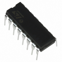
ST7FLITES5Y0B6 STMicroelectronics, ST7FLITES5Y0B6 Datasheet - Page 52

ST7FLITES5Y0B6
Manufacturer Part Number
ST7FLITES5Y0B6
Description
MCU 8BIT 1K FLASH 16DIP
Manufacturer
STMicroelectronics
Series
ST7r
Datasheet
1.ST7FLITES2Y0B6.pdf
(124 pages)
Specifications of ST7FLITES5Y0B6
Core Processor
ST7
Core Size
8-Bit
Speed
8MHz
Connectivity
SPI
Peripherals
LVD, POR, PWM, WDT
Number Of I /o
13
Program Memory Size
1KB (1K x 8)
Program Memory Type
FLASH
Ram Size
128 x 8
Voltage - Supply (vcc/vdd)
2.4 V ~ 5.5 V
Data Converters
A/D 5x10b
Oscillator Type
Internal
Operating Temperature
-40°C ~ 85°C
Package / Case
16-DIP (0.300", 7.62mm)
Processor Series
ST7FLITESx
Core
ST7
Data Bus Width
8 bit
Data Ram Size
128 B
Interface Type
SPI
Maximum Clock Frequency
8 MHz
Number Of Programmable I/os
13
Number Of Timers
2
Operating Supply Voltage
2.4 V to 5.5 V
Maximum Operating Temperature
+ 85 C
Mounting Style
Through Hole
Development Tools By Supplier
ST7FLIT0-IND/USB, ST7FLITE-SK/RAIS, ST7MDT10-DVP3, ST7MDT10-EMU3, STX-RLINK
Minimum Operating Temperature
- 40 C
On-chip Adc
8 bit
For Use With
497-5858 - EVAL BOARD PLAYBACK ST7FLITE497-5049 - KIT STARTER RAISONANCE ST7FLITE
Lead Free Status / RoHS Status
Lead free / RoHS Compliant
Eeprom Size
-
Lead Free Status / Rohs Status
Details
Other names
497-4862
Available stocks
Company
Part Number
Manufacturer
Quantity
Price
ST7LITE0xY0, ST7LITESxY0
LITE TIMER (Cont’d)
11.1.6 Register Description
LITE TIMER CONTROL/STATUS REGISTER
(LTCSR)
Read / Write
Reset Value: 0x00 0000 (x0h)
Bit 7 = ICIE Interrupt Enable
This bit is set and cleared by software.
0: Input Capture (IC) interrupt disabled
1: Input Capture (IC) interrupt enabled
Bit 6 = ICF Input Capture Flag
This bit is set by hardware and cleared by software
by reading the LTICR register. Writing to this bit
does not change the bit value.
0: No input capture
1: An input capture has occurred
Note: After an MCU reset, software must initialise
the ICF bit by reading the LTICR register
Bit 5 = TB Timebase period selection
This bit is set and cleared by software.
0: Timebase period = t
1: Timebase period = t
Bit 4 = TBIE Timebase Interrupt enable
This bit is set and cleared by software.
0: Timebase (TB) interrupt disabled
1: Timebase (TB) interrupt enabled
Bit 3 = TBF Timebase Interrupt Flag
This bit is set by hardware and cleared by software
reading the LTCSR register. Writing to this bit has
no effect.
Table 13. Lite Timer Register Map and Reset Values
52/124
1
ICIE
Address
MHz)
7
(Hex.)
0B
0C
ICF
LTCSR
Reset Value
LTICR
Reset Value
Register
TB
Label
TBIE
OSC
OSC
TBF
* 8000 (1ms @ 8 MHz)
* 16000 (2ms @ 8
ICR7
ICIE
7
0
0
WDGR WDGE WDGD
ICR6
ICF
6
x
0
0
ICR5
TB
5
0
0
0: No counter overflow
1: A counter overflow has occurred
Bit 2 = WDGRF Force Reset/ Reset Status Flag
This bit is used in two ways: it is set by software to
force a watchdog reset. It is set by hardware when
a watchdog reset occurs and cleared by hardware
or by software. It is cleared by hardware only when
an LVD reset occurs. It can be cleared by software
after a read access to the LTCSR register.
0: No watchdog reset occurred.
1: Force a watchdog reset (write), or, a watchdog
Bit 1 = WDGE Watchdog Enable
This bit is set and cleared by software.
0: Watchdog disabled
1: Watchdog enabled
Bit 0 = WDGD Watchdog Reset Delay
This bit is set by software. It is cleared by hard-
ware at the end of each t
0: Watchdog reset not delayed
1: Watchdog reset delayed
LITE TIMER INPUT CAPTURE REGISTER
(LTICR)
Read only
Reset Value: 0000 0000 (00h)
Bit 7:0 = ICR[7:0] Input Capture Value
These bits are read by software and cleared by
hardware after a reset. If the ICF bit in the LTCSR
is cleared, the value of the 8-bit up-counter will be
captured when a rising or falling edge occurs on
the LTIC pin.
ICR7
reset occurred (read).
7
TBIE
ICR4
4
0
0
ICR6
ICR3
TBF
ICR5
3
0
0
ICR4
WDGRF
ICR2
2
0
0
WDG
ICR3
period.
WDGE
ICR2
ICR1
1
0
0
ICR1
WDGD
ICR0
0
0
0
ICR0
0


