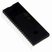
ST72F324J4B5 STMicroelectronics, ST72F324J4B5 Datasheet - Page 12

ST72F324J4B5
Manufacturer Part Number
ST72F324J4B5
Description
MCU 8BIT 16K FLASH 5V 42DIP
Manufacturer
STMicroelectronics
Series
ST7r
Datasheet
1.ST72F324J2T6.pdf
(164 pages)
Specifications of ST72F324J4B5
Core Processor
ST7
Core Size
8-Bit
Speed
8MHz
Connectivity
SCI, SPI
Peripherals
LVD, POR, PWM, WDT
Number Of I /o
32
Program Memory Size
16KB (16K x 8)
Program Memory Type
FLASH
Ram Size
512 x 8
Voltage - Supply (vcc/vdd)
3.8 V ~ 5.5 V
Data Converters
A/D 12x10b
Oscillator Type
Internal
Operating Temperature
-10°C ~ 85°C
Package / Case
42-DIP (0.600", 15.24mm)
Processor Series
ST72F3x
Core
ST7
Data Bus Width
8 bit
Data Ram Size
512 B
Interface Type
SCI, SPI
Maximum Clock Frequency
8 MHz
Number Of Programmable I/os
32
Number Of Timers
2
Maximum Operating Temperature
+ 85 C
Mounting Style
Through Hole
Development Tools By Supplier
ST7F521-IND/USB, ST7232X-EVAL, ST7MDT20-DVP3, ST7MDT20J-EMU3, STX-RLINK
Minimum Operating Temperature
- 10 C
On-chip Adc
10 bit, 12 Channel
For Use With
497-6421 - BOARD EVAL DGTL BATT CHGR DESIGN
Lead Free Status / RoHS Status
Lead free / RoHS Compliant
Eeprom Size
-
Lead Free Status / Rohs Status
Details
Other names
497-4848
Available stocks
Company
Part Number
Manufacturer
Quantity
Price
Company:
Part Number:
ST72F324J4B5
Manufacturer:
STMicroelectronics
Quantity:
135
ST72324Jx ST72324Kx
column (wpu) is merged with the interrupt column (int), then the I/O configuration is pull-up interrupt input,
else the configuration is floating interrupt input.
2. In the open drain output column, “T” defines a true open drain I/O (P-Buffer and protection diode to V
are not implemented). See See “I/O PORTS” on page 45. and
ISTICS
3. OSC1 and OSC2 pins connect a crystal/ceramic resonator, or an external source to the on-chip oscil-
lator; see
more details.
4. On the chip, each I/O port has 8 pads. Pads that are not bonded to external pins are in input pull-up con-
figuration after reset. The configuration of these pads must be kept at reset state to avoid added current
consumption.
5. For details refer to
12/164
1
for more details.
Section 1 INTRODUCTION
Section 12.9.1 on page 133
and
Section 12.6 CLOCK AND TIMING CHARACTERISTICS
Section 12.9 I/O PORT PIN CHARACTER-
DD
for


