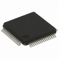
ST72F321BR9T6 STMicroelectronics, ST72F321BR9T6 Datasheet - Page 175

ST72F321BR9T6
Manufacturer Part Number
ST72F321BR9T6
Description
MCU 8BIT 60KB FLASH/ROM 64-LQFP
Manufacturer
STMicroelectronics
Series
ST7r
Datasheet
1.ST72F321BK6T6.pdf
(187 pages)
Specifications of ST72F321BR9T6
Core Processor
ST7
Core Size
8-Bit
Speed
8MHz
Connectivity
I²C, SCI, SPI
Peripherals
LVD, POR, PWM, WDT
Number Of I /o
48
Program Memory Size
60KB (60K x 8)
Program Memory Type
FLASH
Ram Size
2K x 8
Voltage - Supply (vcc/vdd)
3.8 V ~ 5.5 V
Data Converters
A/D 16x10b
Oscillator Type
Internal
Operating Temperature
-40°C ~ 85°C
Package / Case
64-LQFP
Processor Series
ST72F3x
Core
ST7
Data Bus Width
8 bit
Data Ram Size
2 KB
Interface Type
I2C, SCI, SPI
Maximum Clock Frequency
8 MHz
Number Of Programmable I/os
48
Number Of Timers
2
Maximum Operating Temperature
+ 85 C
Mounting Style
SMD/SMT
Development Tools By Supplier
ST7232X-EVAL, ST7232X-SK/RAIS, ST72321B-D/RAIS, ST7MDT20-DVP3, STX-RLINK
Minimum Operating Temperature
- 40 C
On-chip Adc
10 bit, 16 Channel
Cpu Family
ST7
Device Core Size
8b
Frequency (max)
8MHz
Total Internal Ram Size
2KB
# I/os (max)
48
Number Of Timers - General Purpose
2
Operating Supply Voltage (typ)
5V
Operating Supply Voltage (max)
5.5V
Operating Supply Voltage (min)
3.8V
Instruction Set Architecture
CISC
Operating Temp Range
-40C to 85C
Operating Temperature Classification
Industrial
Mounting
Surface Mount
Pin Count
64
Package Type
LQFP
For Use With
497-5046 - KIT TOOL FOR ST7/UPSD/STR7 MCU
Lead Free Status / RoHS Status
Lead free / RoHS Compliant
Eeprom Size
-
Lead Free Status / Rohs Status
Details
Other names
497-5586
Available stocks
Company
Part Number
Manufacturer
Quantity
Price
Company:
Part Number:
ST72F321BR9T6
Manufacturer:
STMicroelectronics
Quantity:
10 000
ST72321B DEVICE CONFIGURATION AND ORDERING INFORMATION (Cont’d)
OPT0= FMP_R Flash memory read-out protection
Read-out protection, when selected, provides a
protection against Program Memory content ex-
traction and against write access to Flash memo-
ry.
Erasing the option bytes when the FMP_R option
is selected causes the whole user memory to be
erased first, and the device can be reprogrammed.
Refer to
gramming Reference Manual for more details.
0: Read-out protection enabled
1: Read-out protection disabled
OPTION BYTE 1
OPT7= PKG1 Package selection bit 1
This option bit selects the package.
Note: On the chip, each I/O port has up to 8 pads.
Pads that are not bonded to external pins are
forced in input pull-up configuration after reset.
The configuration of these pads must be kept at
reset state to avoid added current consumption.
are in input floating configuration after reset. Refer
to Note 4 on
OPT6 = RSTC RESET clock cycle selection
This option bit selects the number of CPU cycles
applied during the RESET phase and when exiting
HALT mode. For resonator oscillators, it is advised
to select 4096 due to the long crystal stabilization
time.
0: Reset phase with 4096 CPU cycles
1: Reset phase with 256 CPU cycles
OPT5:4 = OSCTYPE[1:0] Oscillator Type
These option bits select the ST7 main clock
source type.
Resonator Oscillator
Reserved
Internal RC Oscillator
Version
R/AR
K
J
Clock Source
Section 4.3.1
Selected Package
page
LQFP64
LQFP44
LQFP32
13.
and the ST7 Flash Pro-
Flash size
32/48/60K
48/60K
1
0
0
1
32K
32K
OSCTYPE
ST72321BRx, ST72321BARx ST72321BJx, ST72321BKx
PKG 1
0
0
1
0
1
0
1
0
OPT3:1 = OSCRANGE[2:0] Oscillator range
When the resonator oscillator type is selected,
these option bits select the resonator oscillator
current source corresponding to the frequency
range of the used resonator. Otherwise, these bits
are used to select the normal operating frequency
range.
OPT0 = PLLOFF PLL activation
This option bit activates the PLL which allows mul-
tiplication by two of the main input clock frequency.
The PLL is guaranteed only with an input frequen-
cy between 2 and 4MHz, for this reason the PLL
must not be used with the internal RC oscillator.
0: PLL x2 enabled
1: PLL x2 disabled
CAUTION: the PLL can be enabled only if the
“OSC RANGE” (OPT3:1) bits are configured to “
2~4MHz”. Otherwise, the device functionality is
not guaranteed.
External Source
Typ. Freq. Range
Clock Source
8~16MHz
1~2MHz
2~4MHz
4~8MHz
2
0
0
0
0
OSCRANGE
1
1
OSCTYPE
1
0
0
1
1
175/187
0
1
0
0
1
0
1


