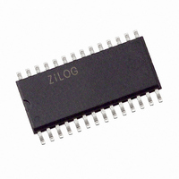
Z86E3412SSG Zilog, Z86E3412SSG Datasheet - Page 63

Z86E3412SSG
Manufacturer Part Number
Z86E3412SSG
Description
IC MICROCONTROLLER 16K 28-SOIC
Manufacturer
Zilog
Series
Z8®r
Datasheet
1.Z86E3312SSC.pdf
(84 pages)
Specifications of Z86E3412SSG
Core Processor
Z8
Core Size
8-Bit
Speed
12MHz
Connectivity
EBI/EMI
Peripherals
POR, WDT
Number Of I /o
24
Program Memory Size
16KB (16K x 8)
Program Memory Type
OTP
Ram Size
237 x 8
Voltage - Supply (vcc/vdd)
3.5 V ~ 5.5 V
Oscillator Type
Internal
Operating Temperature
0°C ~ 70°C
Package / Case
28-SOIC (7.5mm Width)
Processor Series
Z86E3xx
Core
Z8
Data Bus Width
8 bit
Data Ram Size
237 B
Maximum Clock Frequency
12 MHz
Number Of Programmable I/os
24
Number Of Timers
2
Operating Supply Voltage
3.5 V to 5.5 V
Maximum Operating Temperature
+ 70 C
Mounting Style
SMD/SMT
Development Tools By Supplier
Z86E4400ZDV, Z86E4400ZDP, Z86E4400ZDF, Z86E3400ZDV, Z86E3400ZDS, Z86E3400ZDP
Minimum Operating Temperature
0 C
For Use With
309-1073 - ADAPTER 28-SOIC TO 28-SOIC
Lead Free Status / RoHS Status
Lead free / RoHS Compliant
Eeprom Size
-
Data Converters
-
Lead Free Status / Rohs Status
Details
Other names
269-4701-5
Z86E3412SSG
Z86E3412SSG
Available stocks
Company
Part Number
Manufacturer
Quantity
Price
Company:
Part Number:
Z86E3412SSG
Manufacturer:
Zilog
Quantity:
38
PS022901-0508
Figure 31. Stop Mode Recovery Register (Write-Only Except Bit D7, Which Is Read-Only)
** Default setting after RESET and STOP-Mode Recovery
* Default setting after RESET
SCLK/TCLK Divide-by-16 Select (D0). This bit of the SMR controls a divide-by-16
prescaler of SCLK/TCLK. The purpose of this control is to selectively reduce device
power consumption during normal processor execution (SCLK control) and/or HALT
mode (where TCLK sources counter/timers and interrupt logic).
External Clock Divide-by-Two (D1). This bit can eliminate the oscillator divide-by-two
circuitry. When this bit is 0, the System Clock (SCLK) and Timer Clock (TCLK) are equal
to the external clock frequency divided by two. The SCLK/TCLK is equal to the external
clock frequency when this bit is set (D1=1). Using this bit together with D7 of PCON fur-
ther helps lower EMI (that is, D7 (PCON) = 0, D1 (SMR) = 1). The default setting is zero.
Stop Mode Recovery Source (D2, D3, and D4). These three bits of the SMR register
specify the wake up source of the Stop Mode Recovery
SMR source selected with the setting of D2 to D4. P33-P31 cannot be used to wake up
SMR (Fh) 0B
D7 D6 D5
D4 D3 D2 D1
D0
External Clock Divide-by-2
0 SCLK/TCLK = XTAL/2*
1 SCLK/TCLK = XTAL
STOP-Mode Recovery Source
000 POR Only and/or External Reset*
001 P30
010 P31
011 P32
100 P33
101 P27
110 P2 NOR 0-3
111 P2 NOR 0-7
SCLK/TCLK Divide-by-16
0 OFF**
1 ON
Stop Delay
0 OFF
1 ON
Stop Flag (Read only)
0 POR*
1 Stop Recovery
Stop Recovery Level
0 Low*
1 High
CMOS Z8
(Figure
®
32).
Product Specification
OTP Microcontrollers
Electrical Characteristics
Table 22
shows the
59


