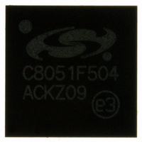
C8051F504-IM Silicon Laboratories Inc, C8051F504-IM Datasheet - Page 143

C8051F504-IM
Manufacturer Part Number
C8051F504-IM
Description
IC 8051 MCU 32K FLASH 48-QFN
Manufacturer
Silicon Laboratories Inc
Series
C8051F50xr
Specifications of C8051F504-IM
Program Memory Type
FLASH
Program Memory Size
32KB (32K x 8)
Package / Case
48-QFN
Mfg Application Notes
LIN Bootloader AppNote
Core Processor
8051
Core Size
8-Bit
Speed
50MHz
Connectivity
EBI/EMI, SMBus (2-Wire/I²C), CAN, LIN, SPI, UART/USART
Peripherals
POR, PWM, Temp Sensor, WDT
Number Of I /o
40
Ram Size
4.25K x 8
Voltage - Supply (vcc/vdd)
1.8 V ~ 5.25 V
Data Converters
A/D 32x12b
Oscillator Type
Internal
Operating Temperature
-40°C ~ 125°C
Processor Series
C8051F5x
Core
8051
Data Bus Width
8 bit
Data Ram Size
4.25 KB
Interface Type
I2C/SPI/UART
Maximum Clock Frequency
50 MHz
Number Of Programmable I/os
40
Number Of Timers
4
Maximum Operating Temperature
+ 125 C
Mounting Style
SMD/SMT
3rd Party Development Tools
PK51, CA51, A51, ULINK2
Development Tools By Supplier
C8051F500DK
Minimum Operating Temperature
- 40 C
On-chip Adc
32-ch x 12-bit
Lead Free Status / RoHS Status
Lead free / RoHS Compliant
For Use With
336-1527 - KIT DEV FOR C8051F50X
Eeprom Size
-
Lead Free Status / Rohs Status
Lead free / RoHS Compliant
Other names
336-1519-5
Available stocks
Company
Part Number
Manufacturer
Quantity
Price
Company:
Part Number:
C8051F504-IM
Manufacturer:
Silicon Labs
Quantity:
135
- Current page: 143 of 312
- Download datasheet (3Mb)
Important Note: If the V
is selected as a reset source. Selecting the V
lized may cause a system reset. In some applications, this reset may be undesirable. If this is not desirable
in the application, a delay should be introduced between enabling the monitor and selecting it as a reset
source. The procedure for enabling the V
state is as follows:
1. Enable the V
2. If necessary, wait for the V
3. Select the V
See Figure 17.2 for V
monitor reset. See Table 5.4 for complete electrical characteristics of the V
See “Figure 5.1. Minimum VDD Monitor Threshold vs. System Clock Frequency” on page 44 for V
itor threshold level requirements.
Note: The output of the internal voltage regulator is calibrated by the MCU immediately after any reset event. The
Note: This delay should be omitted if software contains routines that erase or write Flash
memory.
output of the un-calibrated internal regulator could be below the high threshold setting of the VDD Monitor. If
this is the case and the VDD Monitor is set to the high threshold setting and if the MCU receives a non-power
on reset (POR), the MCU will remain in reset until a POR occurs (i.e., VDD Monitor will keep the device in
reset). A POR will force the VDD Monitor to the low threshold setting which is guaranteed to be below the un-
calibrated output of the internal regulator. The device will then exit reset and resume normal operation. It is for
this reason Silicon Labs strongly recommends that the VDD Monitor is always left in the low threshold setting
(i.e., default value upon POR).
When programming the Flash in-system, the VDD Monitor must be set to the high threshold setting. For the
highest system reliability, the time the VDD Monitor is set to the high threshold setting should be minimized
(e.g. setting the VDD Monitor to the high threshold setting just before the Flash write operation and then
changing it back to the low threshold setting immediately after the Flash write operation).
DD
DD
monitor as a reset source (PORSF bit in RSTSRC = 1).
monitor (VDMEN bit in VDM0CN = 1).
DD
DD
monitor timing; note that the power-on-reset delay is not incurred after a V
monitor is being turned on from a disabled state, it should be enabled before it
DD
monitor to stabilize (see Table 5.4 for the V
DD
monitor and configuring it as a reset source from a disabled
DD
Rev. 1.2
monitor as a reset source before it is enabled and stabi-
C8051F50x/F51x
DD
DD
monitor.
Monitor turn-on time).
DD
mon-
143
DD
Related parts for C8051F504-IM
Image
Part Number
Description
Manufacturer
Datasheet
Request
R
Part Number:
Description:
SMD/C°/SINGLE-ENDED OUTPUT SILICON OSCILLATOR
Manufacturer:
Silicon Laboratories Inc
Part Number:
Description:
Manufacturer:
Silicon Laboratories Inc
Datasheet:
Part Number:
Description:
N/A N/A/SI4010 AES KEYFOB DEMO WITH LCD RX
Manufacturer:
Silicon Laboratories Inc
Datasheet:
Part Number:
Description:
N/A N/A/SI4010 SIMPLIFIED KEY FOB DEMO WITH LED RX
Manufacturer:
Silicon Laboratories Inc
Datasheet:
Part Number:
Description:
N/A/-40 TO 85 OC/EZLINK MODULE; F930/4432 HIGH BAND (REV E/B1)
Manufacturer:
Silicon Laboratories Inc
Part Number:
Description:
EZLink Module; F930/4432 Low Band (rev e/B1)
Manufacturer:
Silicon Laboratories Inc
Part Number:
Description:
I°/4460 10 DBM RADIO TEST CARD 434 MHZ
Manufacturer:
Silicon Laboratories Inc
Part Number:
Description:
I°/4461 14 DBM RADIO TEST CARD 868 MHZ
Manufacturer:
Silicon Laboratories Inc
Part Number:
Description:
I°/4463 20 DBM RFSWITCH RADIO TEST CARD 460 MHZ
Manufacturer:
Silicon Laboratories Inc
Part Number:
Description:
I°/4463 20 DBM RADIO TEST CARD 868 MHZ
Manufacturer:
Silicon Laboratories Inc
Part Number:
Description:
I°/4463 27 DBM RADIO TEST CARD 868 MHZ
Manufacturer:
Silicon Laboratories Inc
Part Number:
Description:
I°/4463 SKYWORKS 30 DBM RADIO TEST CARD 915 MHZ
Manufacturer:
Silicon Laboratories Inc
Part Number:
Description:
N/A N/A/-40 TO 85 OC/4463 RFMD 30 DBM RADIO TEST CARD 915 MHZ
Manufacturer:
Silicon Laboratories Inc
Part Number:
Description:
I°/4463 20 DBM RADIO TEST CARD 169 MHZ
Manufacturer:
Silicon Laboratories Inc


