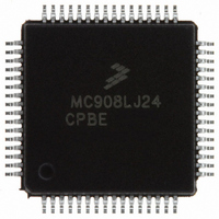
MC908LJ24CPBE Freescale Semiconductor, MC908LJ24CPBE Datasheet - Page 350

MC908LJ24CPBE
Manufacturer Part Number
MC908LJ24CPBE
Description
IC MCU 24K FLASH 8MHZ SPI 64LQFP
Manufacturer
Freescale Semiconductor
Series
HC08r
Datasheet
1.MC908LK24CFUE.pdf
(464 pages)
Specifications of MC908LJ24CPBE
Core Processor
HC08
Core Size
8-Bit
Speed
8MHz
Connectivity
I²C, IRSCI, SPI
Peripherals
LCD, LVD, POR, PWM
Number Of I /o
40
Program Memory Size
24KB (24K x 8)
Program Memory Type
FLASH
Ram Size
768 x 8
Voltage - Supply (vcc/vdd)
3 V ~ 5.5 V
Data Converters
A/D 6x10b
Oscillator Type
Internal
Operating Temperature
-40°C ~ 85°C
Package / Case
64-LQFP
Processor Series
HC08LJ
Core
HC08
Data Bus Width
8 bit
Data Ram Size
768 B
Interface Type
SCI/SPI
Maximum Clock Frequency
8 MHz
Number Of Programmable I/os
48
Number Of Timers
4
Operating Supply Voltage
3.3 V, 5 V
Maximum Operating Temperature
+ 85 C
Mounting Style
SMD/SMT
Development Tools By Supplier
FSICEBASE, M68EML08LJLKE, ZK-HC08LX-A, M68CBL05CE
Minimum Operating Temperature
- 40 C
On-chip Adc
6-ch x 10-bit
Controller Family/series
HC08
No. Of I/o's
40
Ram Memory Size
768Byte
Cpu Speed
8MHz
No. Of Timers
2
Embedded Interface Type
I2C, SCI, SPI
Rohs Compliant
Yes
Lead Free Status / RoHS Status
Lead free / RoHS Compliant
Eeprom Size
-
Lead Free Status / Rohs Status
Lead free / RoHS Compliant
Available stocks
Company
Part Number
Manufacturer
Quantity
Price
Company:
Part Number:
MC908LJ24CPBE
Manufacturer:
Freescale Semiconductor
Quantity:
10 000
Company:
Part Number:
MC908LJ24CPBER
Manufacturer:
Freescale Semiconductor
Quantity:
10 000
- Current page: 350 of 464
- Download datasheet (5Mb)
Liquid Crystal Display (LCD) Driver
17.2 Introduction
17.3 Features
17.4 Pin Name Conventions and I/O Register Addresses
Data Sheet
350
LCD Generic Pin Name
FP11–FP18
FP19–FP26
FP27–FP32
FP1–FP10
BP0–BP2
FP0/BP3
This section describes the liquid crystal display (LCD) driver module.
The LCD driver module can drive a maximum of 33 frontplanes and 4
backplanes, depending on the LCD duty selected.
Features of the LCD driver module include the following:
Three dedicated I/O pins are for the backplanes, BP0–BP2; sixteen
dedicated I/O pins are for the frontplanes, FP1–FP10 and FP27–FP32;
and the sixteen frontplanes, FP11–FP26, are shared with port C and E
pins. FP0 and BP3 shares the same pin and configured by the
DUTY[1:0] bits in the LCD clock register.
The full names of the LCD output pins are shown in
generic pin names appear in the text that follows.
•
•
•
Table 17-1. Pin Name Conventions
Software programmable driver segment configurations:
– 32 frontplanes × 4 backplanes (128 segments)
– 33 frontplanes × 3 backplanes (99 segments)
– 33 frontplanes × 1 backplane (33 segments)
LCD bias voltages generated by internal resistor ladder
Software programmable contrast control
Liquid Crystal Display (LCD) Driver
PTC0/FP19–PTC7/FP26
PTE0/FP11–PTE7/FP18
Full MCU Pin Name
FP27–FP32
FP1–FP10
BP0–BP2
FP0/BP3
Pin Selected for LCD Function by:
PCEL:PCEH in CONFIG2
MC68HC908LJ24/LK24 — Rev. 2.1
PEE in CONFIG2
—
—
—
—
Freescale Semiconductor
Table
17-1. The
Related parts for MC908LJ24CPBE
Image
Part Number
Description
Manufacturer
Datasheet
Request
R
Part Number:
Description:
Manufacturer:
Freescale Semiconductor, Inc
Datasheet:
Part Number:
Description:
Manufacturer:
Freescale Semiconductor, Inc
Datasheet:
Part Number:
Description:
Manufacturer:
Freescale Semiconductor, Inc
Datasheet:
Part Number:
Description:
Manufacturer:
Freescale Semiconductor, Inc
Datasheet:
Part Number:
Description:
Manufacturer:
Freescale Semiconductor, Inc
Datasheet:
Part Number:
Description:
Manufacturer:
Freescale Semiconductor, Inc
Datasheet:
Part Number:
Description:
Manufacturer:
Freescale Semiconductor, Inc
Datasheet:
Part Number:
Description:
Manufacturer:
Freescale Semiconductor, Inc
Datasheet:
Part Number:
Description:
Manufacturer:
Freescale Semiconductor, Inc
Datasheet:
Part Number:
Description:
Manufacturer:
Freescale Semiconductor, Inc
Datasheet:
Part Number:
Description:
Manufacturer:
Freescale Semiconductor, Inc
Datasheet:
Part Number:
Description:
Manufacturer:
Freescale Semiconductor, Inc
Datasheet:
Part Number:
Description:
Manufacturer:
Freescale Semiconductor, Inc
Datasheet:
Part Number:
Description:
Manufacturer:
Freescale Semiconductor, Inc
Datasheet:
Part Number:
Description:
Manufacturer:
Freescale Semiconductor, Inc
Datasheet:


