M30873FHBGP#U3 Renesas Electronics America, M30873FHBGP#U3 Datasheet - Page 340
M30873FHBGP#U3
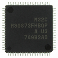
Manufacturer Part Number
M30873FHBGP#U3
Description
IC M32C/87 MCU FLASH 100LQFP
Manufacturer
Renesas Electronics America
Series
M16C™ M32C/80r
Datasheet
1.M3087BFLGPU3.pdf
(629 pages)
Specifications of M30873FHBGP#U3
Core Processor
M32C/80
Core Size
16/32-Bit
Speed
32MHz
Connectivity
EBI/EMI, I²C, IEBus, IrDA, SIO, UART/USART
Peripherals
DMA, POR, PWM, WDT
Number Of I /o
85
Program Memory Size
384KB (384K x 8)
Program Memory Type
FLASH
Ram Size
24K x 8
Voltage - Supply (vcc/vdd)
3 V ~ 5.5 V
Data Converters
A/D 26x10b; D/A 2x8b
Oscillator Type
Internal
Operating Temperature
-40°C ~ 85°C
Package / Case
100-LQFP
For Use With
R0K330879S001BE - KIT DEV RSK M32C/87R0K330879S000BE - KIT DEV RSK M32C/87
Lead Free Status / RoHS Status
Lead free / RoHS Compliant
Eeprom Size
-
Available stocks
Company
Part Number
Manufacturer
Quantity
Price


M32C/87 Group (M32C/87, M32C/87A, M32C/87B)
REJ09B0180-0151 Rev.1.51 Jul 31, 2008
Page 316 of 587
20. CRC Calculation
The CRC (Cyclic Redundancy Check) calculation detects an error in data blocks. A generator polynomial of CRC -
CCITT (X
The CRC code is a 16-bit code generated for a given length of the data block in bytes. The CRC code is stored in the
CRCD register every time one-byte data is transferred to the CRCIN register after a default value is written to the
CRCD register. CRC code generation for one-byte data is completed in two bus clock cycles.
Figure 20.1 shows a block diagram of the CRC circuit. Figure 20.2 shows CRC-associated registers. Figure 20.3
shows an example of the CRC calculation.
Figure 20.1
Figure 20.2
CRC Data Register
CRC Input Register
b15
b7
16
b8 b7
+ X
12
CRC Calculation Block Diagram
CRCD Register, CRCIN Register
+ X
5
b0
b0
+ 1) generates CRC code.
After an initial value is written to the CRCD register, the CRC code
can be read from the CRCD register by writing data to the CRCIN
register. Bit position of the initial value is inverted. The inverted
value is read as the CRC code.
Data input.
Inverse bit position of data
Symbol
CRCD
Symbol
CRCIN
CRCIN register
High-order bits of data bus
Low-order bits of data bus
CRC code generation circuit
Function
Function
8 low-order bits
X
CRCD register
16
+ X
12
Address
037Dh - 037Ch
Adddress
037Eh
+ X
5
+ 1
8 high-order bits
0000h to FFFFh
Setting Range
Setting Range
00h to FFh
After Reset
Undefined
After Reset
Undefined
20. CRC Calculation
RW
RW
RW
RW
Related parts for M30873FHBGP#U3
Image
Part Number
Description
Manufacturer
Datasheet
Request
R

Part Number:
Description:
KIT STARTER FOR M16C/29
Manufacturer:
Renesas Electronics America
Datasheet:

Part Number:
Description:
KIT STARTER FOR R8C/2D
Manufacturer:
Renesas Electronics America
Datasheet:

Part Number:
Description:
R0K33062P STARTER KIT
Manufacturer:
Renesas Electronics America
Datasheet:

Part Number:
Description:
KIT STARTER FOR R8C/23 E8A
Manufacturer:
Renesas Electronics America
Datasheet:

Part Number:
Description:
KIT STARTER FOR R8C/25
Manufacturer:
Renesas Electronics America
Datasheet:

Part Number:
Description:
KIT STARTER H8S2456 SHARPE DSPLY
Manufacturer:
Renesas Electronics America
Datasheet:

Part Number:
Description:
KIT STARTER FOR R8C38C
Manufacturer:
Renesas Electronics America
Datasheet:

Part Number:
Description:
KIT STARTER FOR R8C35C
Manufacturer:
Renesas Electronics America
Datasheet:

Part Number:
Description:
KIT STARTER FOR R8CL3AC+LCD APPS
Manufacturer:
Renesas Electronics America
Datasheet:
Part Number:
Description:
KIT STARTER FOR RX610
Manufacturer:
Renesas Electronics America
Datasheet:

Part Number:
Description:
KIT STARTER FOR R32C/118
Manufacturer:
Renesas Electronics America
Datasheet:

Part Number:
Description:
KIT DEV RSK-R8C/26-29
Manufacturer:
Renesas Electronics America
Datasheet:

Part Number:
Description:
KIT STARTER FOR SH7124
Manufacturer:
Renesas Electronics America
Datasheet:

Part Number:
Description:
KIT STARTER FOR H8SX/1622
Manufacturer:
Renesas Electronics America
Datasheet:

Part Number:
Description:
KIT DEV FOR SH7203
Manufacturer:
Renesas Electronics America
Datasheet: