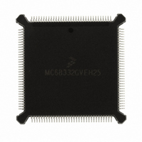
MC68332GVEH25 Freescale Semiconductor, MC68332GVEH25 Datasheet - Page 144

MC68332GVEH25
Manufacturer Part Number
MC68332GVEH25
Description
IC MCU 32BIT 25MHZ 132-PQFP
Manufacturer
Freescale Semiconductor
Series
M683xxr
Specifications of MC68332GVEH25
Core Processor
CPU32
Core Size
32-Bit
Speed
25MHz
Connectivity
EBI/EMI, SCI, SPI, UART/USART
Peripherals
POR, PWM, WDT
Number Of I /o
15
Program Memory Type
ROMless
Ram Size
2K x 8
Voltage - Supply (vcc/vdd)
4.5 V ~ 5.5 V
Oscillator Type
Internal
Operating Temperature
-40°C ~ 105°C
Package / Case
132-QFP
Processor Series
M683xx
Core
CPU32
Data Bus Width
32 bit
Controller Family/series
68K
No. Of I/o's
15
Ram Memory Size
2KB
Cpu Speed
25MHz
No. Of Timers
1
Embedded Interface Type
QSPI, SCI, UART
Digital Ic Case Style
PQFP
Rohs Compliant
Yes
Data Ram Size
2 KB
Interface Type
QSPI, SCI, UART
Maximum Clock Frequency
25 MHz
Number Of Programmable I/os
15
Number Of Timers
16
Maximum Operating Temperature
+ 105 C
Mounting Style
SMD/SMT
Minimum Operating Temperature
- 40 C
Lead Free Status / RoHS Status
Request inventory verification / Request inventory verification
Eeprom Size
-
Program Memory Size
-
Data Converters
-
Lead Free Status / Rohs Status
Lead free / RoHS Compliant
Available stocks
Company
Part Number
Manufacturer
Quantity
Price
Company:
Part Number:
MC68332GVEH25
Manufacturer:
Freescale Semiconductor
Quantity:
135
Company:
Part Number:
MC68332GVEH25
Manufacturer:
Freescale Semiconductor
Quantity:
10 000
- Current page: 144 of 265
- Download datasheet (7Mb)
6.3.5.4 Slave Wraparound Mode
6.3.6 Peripheral Chip Selects
6.4 Serial Communication Interface
6.4.1 SCI Registers
6.4.1.1 Control Registers
6-22
Slave wraparound mode is enabled by setting the WREN bit in SPCR2. The queue can
wrap to pointer address $0 or to the address pointed to by NEWQP, depending on the
state of the WRTO bit in SPCR2. Slave wraparound operation is identical to master
wraparound operation.
Peripheral chip-select signals are used to select an external device for serial data
transfer. Chip-select signals are asserted when a command in the queue is executed.
Signals are asserted at a logic level corresponding to the value of the PCS bits in the
command. More than one chip-select signal can be asserted at a time, and more than
one external device can be connected to each PCS pin, provided proper fanout is ob-
served. PCS0 shares a pin with the slave select SS signal, which initiates slave mode
serial transfer. If SS is taken low when the QSPI is in master mode, a mode fault oc-
curs.
To set up a chip-select function, set the appropriate bit in PQSPAR, then configure the
chip-select pin as an output by setting the appropriate bit in DDRQS. The value of the
bit in PORTQS that corresponds to the chip-select pin determines the base state of
the chip-select signal. If base state is zero, chip-select assertion must be active high
(PCS bit in command RAM must be set); if base state is one, assertion must be active
low (PCS bit in command RAM must be cleared). PORTQS bits are cleared during re-
set. If no new data is written to PORTQS before pin assignment and configuration as
an output, base state of chip-select signals is zero and chip-select pins are configured
for active-high operation.
The serial communication interface (SCI) communicates with external devices through
an asynchronous serial bus. The SCI uses a standard nonreturn to zero (NRZ) trans-
mission format. The SCI is fully compatible with other Freescale SCI systems, such as
those in M68HC11 and M68HC05 devices. Figure 6-7 is a block diagram of the SCI
transmitter; Figure 6-8 is a block diagram of the SCI receiver.
The SCI programming model includes the QSM global and pin control registers, and
four SCI registers. There are two SCI control registers (SCCR0 and SCCR1), one sta-
tus register (SCSR), and one data register (SCDR). Refer to APPENDIX D REGIS-
TER SUMMARY for register bit and field definition.
SCCR0 contains the baud rate selection field. Baud rate must be set before the SCI is
enabled. The CPU can read and write this register at any time.
SCCR1 contains a number of SCI configuration parameters, including transmitter and
receiver enable bits, interrupt enable bits, and operating mode enable bits. The CPU
can read and write this register at any time. The SCI can modify the RWU bit under
certain circumstances.
Freescale Semiconductor, Inc.
For More Information On This Product,
QUEUED SERIAL MODULE
Go to: www.freescale.com
USER’S MANUAL
MC68332
Related parts for MC68332GVEH25
Image
Part Number
Description
Manufacturer
Datasheet
Request
R
Part Number:
Description:
Manufacturer:
Freescale Semiconductor, Inc
Datasheet:
Part Number:
Description:
Manufacturer:
Freescale Semiconductor, Inc
Datasheet:
Part Number:
Description:
Manufacturer:
Freescale Semiconductor, Inc
Datasheet:
Part Number:
Description:
Manufacturer:
Freescale Semiconductor, Inc
Datasheet:
Part Number:
Description:
Manufacturer:
Freescale Semiconductor, Inc
Datasheet:
Part Number:
Description:
Manufacturer:
Freescale Semiconductor, Inc
Datasheet:
Part Number:
Description:
Manufacturer:
Freescale Semiconductor, Inc
Datasheet:
Part Number:
Description:
Manufacturer:
Freescale Semiconductor, Inc
Datasheet:
Part Number:
Description:
Manufacturer:
Freescale Semiconductor, Inc
Datasheet:
Part Number:
Description:
Manufacturer:
Freescale Semiconductor, Inc
Datasheet:
Part Number:
Description:
Manufacturer:
Freescale Semiconductor, Inc
Datasheet:
Part Number:
Description:
Manufacturer:
Freescale Semiconductor, Inc
Datasheet:
Part Number:
Description:
Manufacturer:
Freescale Semiconductor, Inc
Datasheet:
Part Number:
Description:
Manufacturer:
Freescale Semiconductor, Inc
Datasheet:
Part Number:
Description:
Manufacturer:
Freescale Semiconductor, Inc
Datasheet:


