M3087BFLGP#U5 Renesas Electronics America, M3087BFLGP#U5 Datasheet - Page 23
M3087BFLGP#U5
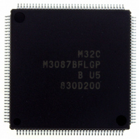
Manufacturer Part Number
M3087BFLGP#U5
Description
IC M32C/87 MCU FLASH 144LQFP
Manufacturer
Renesas Electronics America
Series
M16C™ M32C/80r
Specifications of M3087BFLGP#U5
Core Processor
M32C/80
Core Size
16/32-Bit
Speed
32MHz
Connectivity
CAN, EBI/EMI, I²C, IEBus, IrDA, SIO, UART/USART
Peripherals
DMA, POR, PWM, WDT
Number Of I /o
121
Program Memory Size
1MB (1M x 8)
Program Memory Type
FLASH
Ram Size
48K x 8
Voltage - Supply (vcc/vdd)
3 V ~ 5.5 V
Data Converters
A/D 34x10b, D/A 2x8b
Oscillator Type
Internal
Operating Temperature
-20°C ~ 85°C
Package / Case
144-LQFP
For Use With
R0K330879S001BE - KIT DEV RSK M32C/87R0K330879S000BE - KIT DEV RSK M32C/87
Lead Free Status / RoHS Status
Lead free / RoHS Compliant
Eeprom Size
-
Available stocks
Company
Part Number
Manufacturer
Quantity
Price

Part Number:
M3087BFLGP#U5M3087BFLGP#U3
Manufacturer:
Renesas Electronics America
Quantity:
10 000


M32C/87 Group (M32C/87, M32C/87A, M32C/87B)
REJ03B0127-0151 Rev.1.51 Jul 31, 2008
Page 21 of 85
Table 1.17
I: Input
NOTE:
Intelligent I/O
Reference
voltage input
A/D converter
D/A converter
Real-time port RTP0_0 to
1. Only VCC1 can be used in the 100-pin package.
Type
O: Output
Pin Functions (100-Pin and 144-Pin Package) (3/4)
INPC1_0 to
INPC1_3
INPC1_4 to
INPC1_7
OUTC1_0 to
OUTC1_3
OUTC1_4 to
OUTC1_7
OUTC2_0 to
OUTC2_2
ISCLK0
ISCLK1,
ISCLK2
ISRXD0
ISRXD1,
ISRXD2
ISTXD0
ISTXD1,
ISTXD2
IEIN
IEOUT
VREF
AN_0 to AN_7
AN0_0 to
AN0_7,
AN2_0 to
AN2_7
ADTRG
ANEX0
ANEX1
DA0, DA1
RTP0_3
RTP1_0 to
RTP1_3
RTP2_0 to
RTP2_3
RTP3_0 to
RTP3_3
Symbol
I/O: Input and output
Type
I/O
I/O
I/O
I/O
O
O
O
O
O
O
O
O
I
I
I
I
I
I
I
I
I
I
VCC2
VCC2
VCC2
VCC2
VCC2
VCC2
VCC2
VCC2
Voltage
Supply
VCC1/
VCC1/
VCC1/
VCC1/
VCC1/
VCC1/
VCC1/
VCC1/
VCC1
VCC1
VCC1
VCC1
VCC1
VCC1
VCC2
VCC1
VCC1
VCC1
VCC1
VCC1
−
(1)
(1)
(1)
(1)
(1)
(1)
(1)
(1)
Input pins for the time measurement function.
Output pins for the waveform generation function.
(OUTC1_6/OUTC2_0 and OUTC1_7/OUTC2_2 assigned to ports
7_0 and 7_1 are N-channel open drain output.)
Clock input/output pins for the intelligent I/O communication
function.
Data input pins for the intelligent I/O communication function.
Data output pins for the intelligent I/O communication function.
(ISTXD2 assigned to port 7_0 is N-channel open drain output.)
Data input pin for the intelligent I/O communication function.
Data output pin for the intelligent I/O communication function.
(IEOUT assigned to port 7_0 is N-channel open drain output.)
The VREF pin supplies the reference voltage to the A/D converter
and D/A converter.
Analog input pins for the A/D converter.
External trigger input pin for the A/D converter.
Extended analog input pin for the A/D converter or output pin in
external op-amp connection mode.
Extended analog input pin for the A/D converter.
Output pins for the D/A converter.
These pins function as real-time ports.
(RTP0_2 and RTP0_3 are N-channel open drain output.)
Description
1. Overview
Related parts for M3087BFLGP#U5
Image
Part Number
Description
Manufacturer
Datasheet
Request
R

Part Number:
Description:
KIT STARTER FOR M16C/29
Manufacturer:
Renesas Electronics America
Datasheet:

Part Number:
Description:
KIT STARTER FOR R8C/2D
Manufacturer:
Renesas Electronics America
Datasheet:

Part Number:
Description:
R0K33062P STARTER KIT
Manufacturer:
Renesas Electronics America
Datasheet:

Part Number:
Description:
KIT STARTER FOR R8C/23 E8A
Manufacturer:
Renesas Electronics America
Datasheet:

Part Number:
Description:
KIT STARTER FOR R8C/25
Manufacturer:
Renesas Electronics America
Datasheet:

Part Number:
Description:
KIT STARTER H8S2456 SHARPE DSPLY
Manufacturer:
Renesas Electronics America
Datasheet:

Part Number:
Description:
KIT STARTER FOR R8C38C
Manufacturer:
Renesas Electronics America
Datasheet:

Part Number:
Description:
KIT STARTER FOR R8C35C
Manufacturer:
Renesas Electronics America
Datasheet:

Part Number:
Description:
KIT STARTER FOR R8CL3AC+LCD APPS
Manufacturer:
Renesas Electronics America
Datasheet:
Part Number:
Description:
KIT STARTER FOR RX610
Manufacturer:
Renesas Electronics America
Datasheet:

Part Number:
Description:
KIT STARTER FOR R32C/118
Manufacturer:
Renesas Electronics America
Datasheet:

Part Number:
Description:
KIT DEV RSK-R8C/26-29
Manufacturer:
Renesas Electronics America
Datasheet:

Part Number:
Description:
KIT STARTER FOR SH7124
Manufacturer:
Renesas Electronics America
Datasheet:

Part Number:
Description:
KIT STARTER FOR H8SX/1622
Manufacturer:
Renesas Electronics America
Datasheet:

Part Number:
Description:
KIT DEV FOR SH7203
Manufacturer:
Renesas Electronics America
Datasheet: