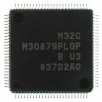
M30879FLGP#U3 Renesas Electronics America, M30879FLGP#U3 Datasheet - Page 24

M30879FLGP#U3
Manufacturer Part Number
M30879FLGP#U3
Description
IC M32C/87 MCU FLASH 100LQFP
Manufacturer
Renesas Electronics America
Series
M16C™ M32C/80r
Specifications of M30879FLGP#U3
Core Size
16/32-Bit
Program Memory Size
1MB (1M x 8)
Core Processor
M32C/80
Speed
32MHz
Connectivity
CAN, EBI/EMI, I²C, IEBus, IrDA, SIO, UART/USART
Peripherals
DMA, POR, PWM, WDT
Number Of I /o
85
Program Memory Type
FLASH
Ram Size
48K x 8
Voltage - Supply (vcc/vdd)
3 V ~ 5.5 V
Data Converters
A/D 26x10b; D/A 2x8b
Oscillator Type
Internal
Operating Temperature
-40°C ~ 85°C
Package / Case
100-LQFP
Controller Family/series
M32C
No. Of I/o's
85
Ram Memory Size
48KB
Cpu Speed
32MHz
No. Of Timers
2
Digital Ic Case Style
LQFP
Embedded Interface Type
CAN, I2C, UART
Rohs Compliant
Yes
Lead Free Status / RoHS Status
Lead free / RoHS Compliant
For Use With
R0K330879S001BE - KIT DEV RSK M32C/87R0K330879S000BE - KIT DEV RSK M32C/87
Eeprom Size
-
Lead Free Status / RoHS Status
Lead free / RoHS Compliant, Lead free / RoHS Compliant
Available stocks
Company
Part Number
Manufacturer
Quantity
Price
Part Number:
M30879FLGP#U3M30879FLGP#U5
Manufacturer:
Renesas Electronics America
Quantity:
10 000
M32C/87 Group (M32C/87, M32C/87A, M32C/87B)
REJ03B0127-0151 Rev.1.51 Jul 31, 2008
Page 22 of 85
Table 1.18
I: Input
Table 1.19
I: Input
I/O port
Input port
Key input
interrupt input
INT Interrupt
Input
Serial
interface
Intelligent I/O
A/D converter
I/O port
Type
Type
O: Output
O: Output
Pin Functions (100-Pin and 144-Pin Package) (4/4)
Pin Functions (144-Pin Package Only)
P0_0 to P0_7,
P1_0 to P1_7,
P2_0 to P2_7,
P3_0 to P3_7,
P4_0 to P4_7,
P5_0 to P5_7
P6_0 to P6_7,
P7_0 to P7_7,
P9_0 to P9_7,
P10_0 to
P10_7
P8_0 to P8_4
P8_6, P8_7
P8_5
KI0 to KI3
INT6 to INT8
CTS6
RTS6
CLK6
RXD6
TXD6
OUTC2_3 to
OUTC2_7
AN15_0 to
AN15_7
P11_0 to
P11_4,
P12_0 to
P12_7,
P13_0 to
P13_7
P14_0 to
P14_6,
P15_0 to
P15_7
Symbol
Symbol
I/O: Input and output
I/O: Input and output
Type
Type
I/O
I/O
I/O
I/O
I/O
I/O
I/O
I/O
O
O
O
I
I
I
I
I
I
Voltage
Voltage
Supply
Supply
VCC1/
VCC1/
VCC1/
VCC1/
VCC1/
VCC2
VCC1
VCC1
VCC1
VCC1
VCC1
VCC2
VCC2
VCC2
VCC2
VCC2
VCC2
VCC1
VCC2
VCC1
8-bit CMOS I/O ports. The Port Pi Direction Register (i = 0 to 15)
determines if each pin is used as an input port or an output port.
The Pull-Up Control Registers determine if the input ports, divided
into groups of four, are pulled up or not.
These 8-bit I/O ports are functionally equivalent to P0.
(P7_0 and P7_1 are N-channel open drain output.)
These I/O ports are functionally equivalent to P0.
Shares the pin with NMI. Input port to read NMI pin level.
Key input interrupt input pins.
INT interrupt input pins.
Input pin to control data transmission.
Output pin to control data reception.
Serial clock input/output pin.
Serial data input pin.
Serial data output pin.
Output pins for the waveform generation function.
Analog input pins for the A/D converter.
These I/O ports are functionally equivalent to P0.
These I/O ports are functionally equivalent to P0.
Description
Description
1. Overview


