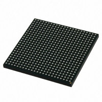
MCIMX513DJM8C Freescale Semiconductor, MCIMX513DJM8C Datasheet - Page 76

MCIMX513DJM8C
Manufacturer Part Number
MCIMX513DJM8C
Description
MULTIMEDIA PROC 529-LFBGA
Manufacturer
Freescale Semiconductor
Series
i.MX51r
Specifications of MCIMX513DJM8C
Core Processor
ARM Cortex-A8
Core Size
32-Bit
Speed
800MHz
Connectivity
1-Wire, EBI/EMI, Ethernet, I²C, IrDA, MMC, SPI, SSI, UART/USART, USB OTG
Peripherals
DMA, I²S, LCD, POR, PWM, WDT
Number Of I /o
128
Program Memory Type
ROMless
Ram Size
128K x 8
Voltage - Supply (vcc/vdd)
0.8 V ~ 1.15 V
Oscillator Type
External
Operating Temperature
-20°C ~ 85°C
Package / Case
529-LFBGA
Processor Series
i.MX51
Core
ARM Cortex A8
Data Bus Width
32 bit
Program Memory Size
36 KB
Data Ram Size
128 KB
Interface Type
I2C, SPI, SSI, UART, USB
Maximum Clock Frequency
200 MHz
Number Of Timers
5
Operating Supply Voltage
0.8 V to 1.15 V
Maximum Operating Temperature
+ 85 C
Mounting Style
SMD/SMT
3rd Party Development Tools
MDK-ARM, RL-ARM, ULINK2
Development Tools By Supplier
MCIMX51EVKJ
Minimum Operating Temperature
- 20 C
Lead Free Status / RoHS Status
Lead free / RoHS Compliant
Eeprom Size
-
Program Memory Size
-
Data Converters
-
Lead Free Status / Rohs Status
Lead free / RoHS Compliant
- Current page: 76 of 200
- Download datasheet (6Mb)
1
Electrical Characteristics
4.7.4
This section describes the electrical information of the Fast Ethernet Controller (FEC) module. The FEC
is designed to support both 10 and 100 Mbps Ethernet/IEEE 802.3 networks. An external transceiver
interface and transceiver function are required to complete the interface to the media. The FEC supports
the 10/100 Mbps MII (18 pins in total) and the 10 Mbps-only 7-wire interface, which uses 7 of the MII
pins, for connection to an external Ethernet transceiver. For the pin list of MII and 7-wire, refer to the
i.MX51 Multimedia Applications Processor Reference Manual (MCIMX51RM).
This section describes the AC timing specifications of the FEC.
4.7.4.1
The MII receive signal timing involves the FEC_RXD[3:0], FEC_RX_DV, FEC_RX_ER, and
FEC_RX_CLK signals. The receiver functions correctly up to a FEC_RX_CLK maximum frequency of
25 MHz + 1%. There is no minimum frequency requirement but the processor clock frequency must
exceed twice the FEC_RX_CLK frequency.
parameters and
76
1
2
3
4
5
.
Num
FEC_RX_DV, FEC_RX_CLK, and FEC_RXD0 have same timing in 10 Mbps 7-wire interface mode.
SD7
SD8
In low speed mode, card clock must be lower than 400 kHz, voltage ranges from 2.7 to 3.6 V.
In normal speed mode for SD/SDIO card, clock frequency can be any value between 0
frequency can be any value between 0
In normal speed mode for MMC card, clock frequency can be any value between 0
frequency can be any value between 0
Measurement taken with CLoad = 20 pF
To satisfy hold timing, the delay difference between clock input and cmd/data input must not exceed 2 ns.
M1
M2
M3
M4
ID
eSDHC Input Setup Time
eSDHC Input Hold Time
FEC_RXD[3:0], FEC_RX_DV, FEC_RX_ER to FEC_RX_CLK setup
FEC_RX_CLK to FEC_RXD[3:0], FEC_RX_DV, FEC_RX_ER hold
FEC_RX_CLK pulse width high
FEC_RX_CLK pulse width low
FEC AC Timing Parameters
MII Receive Signal Timing
Figure 42
i.MX51 Applications Processors for Consumer and Industrial Products, Rev. 4
Table 69. eSDHCv2 Interface Timing Specification (continued)
shows MII receive signal timings.
Parameter
Characteristic
–
–
Table 70. MII Receive Signal Timing
50 MHz.
52 MHz.
1
Table 70
lists the MII receive channel signal timing
Symbols
t
t
ISU
IH
5
35%
35%
Min
5
5
–
20 MHz. In high-speed mode, clock
–
25 MHz. In high-speed mode, clock
Min
2.5
2.5
Max
65%
65%
—
—
Freescale Semiconductor
FEC_RX_CLK period
FEC_RX_CLK period
Max
—
—
Unit
ns
ns
Unit
ns
ns
Related parts for MCIMX513DJM8C
Image
Part Number
Description
Manufacturer
Datasheet
Request
R
Part Number:
Description:
MCIMX-LVDS1
Manufacturer:
Freescale Semiconductor
Datasheet:
Part Number:
Description:
Manufacturer:
Freescale Semiconductor, Inc
Datasheet:
Part Number:
Description:
Manufacturer:
Freescale Semiconductor, Inc
Datasheet:
Part Number:
Description:
Manufacturer:
Freescale Semiconductor, Inc
Datasheet:
Part Number:
Description:
Manufacturer:
Freescale Semiconductor, Inc
Datasheet:
Part Number:
Description:
Manufacturer:
Freescale Semiconductor, Inc
Datasheet:
Part Number:
Description:
Manufacturer:
Freescale Semiconductor, Inc
Datasheet:
Part Number:
Description:
Manufacturer:
Freescale Semiconductor, Inc
Datasheet:
Part Number:
Description:
Manufacturer:
Freescale Semiconductor, Inc
Datasheet:
Part Number:
Description:
Manufacturer:
Freescale Semiconductor, Inc
Datasheet:
Part Number:
Description:
Manufacturer:
Freescale Semiconductor, Inc
Datasheet:
Part Number:
Description:
Manufacturer:
Freescale Semiconductor, Inc
Datasheet:
Part Number:
Description:
Manufacturer:
Freescale Semiconductor, Inc
Datasheet:
Part Number:
Description:
Manufacturer:
Freescale Semiconductor, Inc
Datasheet:
Part Number:
Description:
Manufacturer:
Freescale Semiconductor, Inc
Datasheet:


