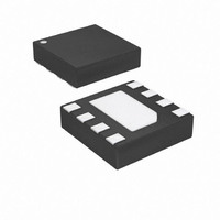
ATTINY5-MAHR Atmel, ATTINY5-MAHR Datasheet - Page 62

ATTINY5-MAHR
Manufacturer Part Number
ATTINY5-MAHR
Description
IC MCU AVR 512B FLASH 8UDFN
Manufacturer
Atmel
Series
AVR® ATtinyr
Datasheet
1.ATTINY9-MAHR.pdf
(169 pages)
Specifications of ATTINY5-MAHR
Package / Case
8-UDFN Exposed Pad
Voltage - Supply (vcc/vdd)
1.8 V ~ 5.5 V
Operating Temperature
-40°C ~ 85°C
Speed
12MHz
Number Of I /o
4
Core Processor
AVR
Program Memory Type
FLASH
Ram Size
32 x 8
Program Memory Size
512B (512 x 8)
Data Converters
A/D 4x8b
Oscillator Type
Internal
Peripherals
POR, PWM, WDT
Core Size
8-Bit
Lead Free Status / RoHS Status
Lead free / RoHS Compliant
Eeprom Size
-
Connectivity
-
Lead Free Status / Rohs Status
Details
- Current page: 62 of 169
- Download datasheet (5Mb)
11.7
62
Compare Match Output Unit
ATtiny4/5/9/10
The Compare Output Mode (COM0x1:0) bits have two functions. The Waveform Generator uses
the COM0x1:0 bits for defining the Output Compare (OC0x) state at the next compare match.
Secondly the COM0x1:0 bits control the OC0x pin output source.
a simplified schematic of the logic affected by the COM0x1:0 bit setting. The I/O Registers, I/O
bits, and I/O pins in the figure are shown in bold. Only the parts of the general I/O port control
registers (DDR and PORT) that are affected by the COM0x1:0 bits are shown. When referring to
the OC0x state, the reference is for the internal OC0x Register, not the OC0x pin. If a system
reset occur, the OC0x Register is reset to “0”.
Figure 11-7. Compare Match Output Unit, Schematic (non-PWM Mode)
The general I/O port function is overridden by the Output Compare (OC0x) from the Waveform
Generator if either of the COM0x1:0 bits are set. However, the OC0x pin direction (input or out-
put) is still controlled by the Data Direction Register (DDR) for the port pin. The Data Direction
Register bit for the OC0x pin (DDR_OC0x) must be set as output before the OC0x value is visi-
ble on the pin. The port override function is generally independent of the Waveform Generation
mode, but there are some exceptions. See
Table 11-4 on page 75
The design of the Output Compare pin logic allows initialization of the OC0x state before the out-
put is enabled. Note that some COM0x1:0 bit settings are reserved for certain modes of
operation. See
The COM0x1:0 bits have no effect on the Input Capture unit.
COMnx1
COMnx0
FOCnx
clk
I/O
“Register Description” on page 74
Waveform
Generator
for details.
D
D
D
PORT
DDR
OCnx
Table 11-2 on page
Q
Q
Q
75,
1
0
Figure 11-7 on page 62
Table 11-3 on page 75
8127D–AVR–02/10
OCnx
Pin
shows
and
Related parts for ATTINY5-MAHR
Image
Part Number
Description
Manufacturer
Datasheet
Request
R

Part Number:
Description:
Manufacturer:
Atmel Corporation
Datasheet:

Part Number:
Description:
IC MCU AVR 512B FLASH SOT-23-6
Manufacturer:
Atmel
Datasheet:

Part Number:
Description:
IC MCU AVR 512B FLASH SOT-23-6
Manufacturer:
Atmel
Datasheet:

Part Number:
Description:
IC MCU AVR 512B FLASH 8UDFN
Manufacturer:
Atmel
Datasheet:

Part Number:
Description:
DEV KIT FOR AVR/AVR32
Manufacturer:
Atmel
Datasheet:

Part Number:
Description:
INTERVAL AND WIPE/WASH WIPER CONTROL IC WITH DELAY
Manufacturer:
ATMEL Corporation
Datasheet:

Part Number:
Description:
Low-Voltage Voice-Switched IC for Hands-Free Operation
Manufacturer:
ATMEL Corporation
Datasheet:

Part Number:
Description:
MONOLITHIC INTEGRATED FEATUREPHONE CIRCUIT
Manufacturer:
ATMEL Corporation
Datasheet:

Part Number:
Description:
AM-FM Receiver IC U4255BM-M
Manufacturer:
ATMEL Corporation
Datasheet:

Part Number:
Description:
Monolithic Integrated Feature Phone Circuit
Manufacturer:
ATMEL Corporation
Datasheet:

Part Number:
Description:
Multistandard Video-IF and Quasi Parallel Sound Processing
Manufacturer:
ATMEL Corporation
Datasheet:

Part Number:
Description:
High-performance EE PLD
Manufacturer:
ATMEL Corporation
Datasheet:


