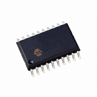
PIC16F631-E/SO Microchip Technology, PIC16F631-E/SO Datasheet - Page 179

PIC16F631-E/SO
Manufacturer Part Number
PIC16F631-E/SO
Description
IC PIC MCU FLASH 1KX14 20SOIC
Manufacturer
Microchip Technology
Series
PIC® 16Fr
Datasheets
1.PIC16F616T-ISL.pdf
(8 pages)
2.PIC16F690DM-PCTLHS.pdf
(306 pages)
3.PIC16F677-IP.pdf
(2 pages)
4.PIC16F677-IP.pdf
(16 pages)
Specifications of PIC16F631-E/SO
Core Processor
PIC
Core Size
8-Bit
Speed
20MHz
Peripherals
Brown-out Detect/Reset, POR, WDT
Number Of I /o
18
Program Memory Size
1.75KB (1K x 14)
Program Memory Type
FLASH
Eeprom Size
128 x 8
Ram Size
64 x 8
Voltage - Supply (vcc/vdd)
2 V ~ 5.5 V
Oscillator Type
Internal
Operating Temperature
-40°C ~ 125°C
Package / Case
20-SOIC (7.5mm Width)
For Use With
658-1047-5 - BOARD EVALUATION ACCESSTOUCHAC162061 - HEADER INTRFC MPLAB ICD2 20PINAC164039 - MODULE SKT PROMATE II 20DIP/SOIC
Lead Free Status / RoHS Status
Lead free / RoHS Compliant
Data Converters
-
Connectivity
-
- PIC16F616T-ISL PDF datasheet
- PIC16F690DM-PCTLHS PDF datasheet #2
- PIC16F677-IP PDF datasheet #3
- PIC16F677-IP PDF datasheet #4
- Current page: 179 of 306
- Download datasheet (6Mb)
12.5
The EUSART WILL remain active during Sleep only in
the Synchronous Slave mode. All other modes require
the system clock and therefore cannot generate the
necessary signals to run the Transmit or Receive Shift
registers during Sleep.
Synchronous Slave mode uses an externally generated
clock to run the Transmit and Receive Shift registers.
12.5.1
To receive during Sleep, all the following conditions
must be met before entering Sleep mode:
• RCSTA and TXSTA Control registers must be
• If interrupts are desired, set the RCIE bit of the
• The RCIF interrupt flag must be cleared by read-
Upon entering Sleep mode, the device will be ready to
accept data and clocks on the RX/DT and TX/CK pins,
respectively. When the data word has been completely
clocked in by the external device, the RCIF interrupt
flag bit of the PIR1 register will be set. Thereby, waking
the processor from Sleep.
Upon waking from Sleep, the instruction following the
SLEEP instruction will be executed. If the GIE Global
Interrupt Enable bit of the INTCON register is also set,
then the Interrupt Service Routine at address 004h will
be called.
© 2008 Microchip Technology Inc.
configured for Synchronous Slave Reception (see
Section 12.4.2.4 “Synchronous Slave
Reception Set-up:”).
PIE1 register and the GIE and PEIE bits of the
INTCON register.
ing RCREG to unload any pending characters in
the receive buffer.
EUSART Operation During Sleep
SYNCHRONOUS RECEIVE DURING
SLEEP
PIC16F631/677/685/687/689/690
12.5.2
To transmit during Sleep, all the following conditions
must be met before entering Sleep mode:
• RCSTA and TXSTA Control registers must be
• The TXIF interrupt flag must be cleared by writing
9.
• Interrupt enable bits TXIE of the PIE1 register and
Upon entering Sleep mode, the device will be ready to
accept clocks on TX/CK pin and transmit data on the
RX/DT pin. When the data word in the TSR has been
completely clocked out by the external device, the
pending byte in the TXREG will transfer to the TSR and
the TXIF flag will be set. Thereby, waking the processor
from Sleep. At this point, the TXREG is available to
accept another character for transmission, which will
clear the TXIF flag.
Upon waking from Sleep, the instruction following the
SLEEP instruction will be executed. If the GIE Global
Interrupt Enable bit is also set then the Interrupt
Service Routine at address 0004h will be called.
configured for Synchronous Slave Transmission
(see Section 12.4.2.2 “Synchronous Slave
Transmission Set-up:”).
the output data to the TXREG, thereby filling the
TSR and transmit buffer.
PEIE of the INTCON register must set.
If interrupts are desired, set the TXIE bit of the
PIE1 register and the PEIE bit of the INTCON
register.
SYNCHRONOUS TRANSMIT
DURING SLEEP
DS41262E-page 177
Related parts for PIC16F631-E/SO
Image
Part Number
Description
Manufacturer
Datasheet
Request
R

Part Number:
Description:
IC PIC MCU FLASH 1KX14 20SSOP
Manufacturer:
Microchip Technology
Datasheet:

Part Number:
Description:
IC PIC MCU FLASH 1KX14 20DIP
Manufacturer:
Microchip Technology
Datasheet:

Part Number:
Description:
IC PIC MCU FLASH 1KX14 20DIP
Manufacturer:
Microchip Technology
Datasheet:

Part Number:
Description:
IC PIC MCU FLASH 1KX14 20SOIC
Manufacturer:
Microchip Technology
Datasheet:

Part Number:
Description:
IC,MICROCONTROLLER,8-BIT,PIC CPU,CMOS,LLCC,20PIN,PLASTIC
Manufacturer:
Microchip Technology
Datasheet:

Part Number:
Description:
IC,MICROCONTROLLER,8-BIT,PIC CPU,CMOS,SSOP,20PIN,PLASTIC
Manufacturer:
Microchip Technology
Datasheet:

Part Number:
Description:
IC,MICROCONTROLLER,8-BIT,PIC CPU,CMOS,LLCC,20PIN,PLASTIC
Manufacturer:
Microchip Technology
Datasheet:

Part Number:
Description:
IC, 8BIT MCU, PIC16F, 32MHZ, SOIC-18
Manufacturer:
Microchip Technology
Datasheet:

Part Number:
Description:
IC, 8BIT MCU, PIC16F, 32MHZ, SSOP-20
Manufacturer:
Microchip Technology
Datasheet:

Part Number:
Description:
IC, 8BIT MCU, PIC16F, 32MHZ, DIP-18
Manufacturer:
Microchip Technology
Datasheet:

Part Number:
Description:
IC, 8BIT MCU, PIC16F, 32MHZ, QFN-28
Manufacturer:
Microchip Technology
Datasheet:

Part Number:
Description:
IC, 8BIT MCU, PIC16F, 32MHZ, QFN-28
Manufacturer:
Microchip Technology
Datasheet:

Part Number:
Description:
IC, 8BIT MCU, PIC16F, 32MHZ, QFN-28
Manufacturer:
Microchip Technology
Datasheet:

Part Number:
Description:
IC, 8BIT MCU, PIC16F, 32MHZ, SSOP-20
Manufacturer:
Microchip Technology
Datasheet:

Part Number:
Description:
IC, 8BIT MCU, PIC16F, 20MHZ, DIP-40
Manufacturer:
Microchip Technology
Datasheet:


