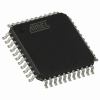
AT80C51RD2-RLRUM Atmel, AT80C51RD2-RLRUM Datasheet - Page 5

AT80C51RD2-RLRUM
Manufacturer Part Number
AT80C51RD2-RLRUM
Description
IC MCU 80C51 HI PERFORM 44VQFP
Manufacturer
Atmel
Series
80Cr
Datasheet
1.AT80C51RD2-RLRUM.pdf
(81 pages)
Specifications of AT80C51RD2-RLRUM
Core Processor
8051
Core Size
8-Bit
Speed
40MHz
Connectivity
UART/USART
Peripherals
POR, PWM, WDT
Number Of I /o
32
Program Memory Type
ROMless
Ram Size
1K x 8
Voltage - Supply (vcc/vdd)
2.7 V ~ 5.5 V
Oscillator Type
Internal
Operating Temperature
-40°C ~ 85°C
Package / Case
44-TQFP, 44-VQFP
Processor Series
AT80x
Core
8051
Data Bus Width
8 bit
Data Ram Size
1280 B
Interface Type
UART, SPI
Maximum Clock Frequency
60 MHz
Number Of Programmable I/os
32
Number Of Timers
3
Operating Supply Voltage
2.7 V to 5.5 V
Maximum Operating Temperature
+ 85 C
Mounting Style
SMD/SMT
3rd Party Development Tools
PK51, CA51, A51, ULINK2
Minimum Operating Temperature
- 40 C
Lead Free Status / RoHS Status
Lead free / RoHS Compliant
Eeprom Size
-
Program Memory Size
-
Data Converters
-
Lead Free Status / Rohs Status
Details
Available stocks
Company
Part Number
Manufacturer
Quantity
Price
Company:
Part Number:
AT80C51RD2-RLRUM
Manufacturer:
NXP
Quantity:
8 243
Table 3-1.
4113D–8051–01/09
Mnemonic
P2.0 - P2.7
P3.0 - P3.7
RST
ALE/PROG
PSEN
EA
Pin Description (Continued)
21 - 28
10 - 17
DIL
10
11
12
13
14
15
16
17
30
29
31
9
PLCC44
24 - 31
13 - 19
Pin Number
11,
11
13
14
15
16
17
18
19
10
33
32
35
VQFP44 1.4
18 - 25
7 - 13
10
11
12
13
27
26
29
5,
5
7
8
9
4
Type
O (I)
I/O
I/O
I/O
O
O
O
O
I
I
I
I
I
I
Name and Function
Port 2: Port 2 is an 8-bit bi-directional I/O port with internal pull-ups. Port 2 pins
that have 1s written to them are pulled high by the internal pull-ups and can be
used as inputs. As inputs, Port 2 pins that are externally pulled low will source
current because of the internal pull-ups. Port 2 emits the high-order address byte
during fetches from external program memory and during accesses to external
data memory that use 16-bit addresses (MOVX @DPTR). In this application, it
uses strong internal pull-ups emitting 1s. During accesses to external data memory
that use 8-bit addresses (MOVX @Ri), Port 2 emits the contents of the P2 SFR.
Some Port 2 pins receive the high order address bits during ROM reading and
verification:
P2.0 to P2.5 for 16 KB devices
P2.0 to P2.6 for 32 KB devices
Port 3: Port 3 is an 8-bit bi-directional I/O port with internal pull-ups. Port 3 pins
that have 1s written to them are pulled high by the internal pull-ups and can be
used as inputs. As inputs, Port 3 pins that are externally pulled low will source
current because of the internal pull-ups. Port 3 also serves the special features of
the 80C51 family, as listed below.
RXD (P3.0): Serial input port
TXD (P3.1): Serial output port
INT0 (P3.2): External interrupt 0
INT1 (P3.3): External interrupt 1
T0 (P3.4): Timer 0 external input
T1 (P3.5): Timer 1 external input
WR (P3.6): External data memory write strobe
RD (P3.7): External data memory read strobe
Reset: A high on this pin for two machine cycles while the oscillator is running,
resets the device. An internal diffused resistor to V
using only an external capacitor to V
watchdog forces a system reset.
Address Latch Enable/Program Pulse: Output pulse for latching the low byte of
the address during an access to external memory. In normal operation, ALE is
emitted at a constant rate of 1/6 (1/3 in X2 mode) the oscillator frequency, and can
be used for external timing or clocking. Note that one ALE pulse is skipped during
each access to external data memory. This pin is also the program pulse input
(PROG) during Flash programming. ALE can be disabled by setting SFR’s AUXR.0
bit. With this bit set, ALE will be inactive during internal fetches.
Program Strobe Enable: The read strobe to external program memory. When
executing code from the external program memory, PSEN is activated twice each
machine cycle, except that two PSEN activations are skipped during each access
to external data memory. PSEN is not activated during fetches from internal
program memory.
External Access Enable: EA must be externally held low to enable the device to
fetch code from external program memory locations. If security level 1 is
programmed, EA will be internally latched on Reset.
CC
. This pin is an output when the hardware
SS
AT80C51RD2
permits a power-on reset
5


