PIC16LF723A-I/ML Microchip Technology, PIC16LF723A-I/ML Datasheet - Page 258
PIC16LF723A-I/ML
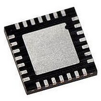
Manufacturer Part Number
PIC16LF723A-I/ML
Description
MCU PIC 3.5K FLASH XLP 28-QFN
Manufacturer
Microchip Technology
Series
PIC® XLP™ 16Fr
Specifications of PIC16LF723A-I/ML
Core Size
8-Bit
Program Memory Size
7KB (4K x 14)
Peripherals
Brown-out Detect/Reset, POR, PWM, WDT
Core Processor
PIC
Speed
20MHz
Connectivity
I²C, SPI, UART/USART
Number Of I /o
25
Program Memory Type
FLASH
Ram Size
192 x 8
Voltage - Supply (vcc/vdd)
1.8 V ~ 3.6 V
Data Converters
A/D 11x8b
Oscillator Type
Internal
Operating Temperature
-40°C ~ 85°C
Package / Case
28-VQFN Exposed Pad, 28-HVQFN, 28-SQFN, 28-DHVQFN
Controller Family/series
PIC16LF
No. Of I/o's
25
Ram Memory Size
192Byte
Cpu Speed
20MHz
No. Of Timers
3
Lead Free Status / RoHS Status
Lead free / RoHS Compliant
Eeprom Size
-
Lead Free Status / RoHS Status
Lead free / RoHS Compliant, Lead free / RoHS Compliant


PIC16F72X/PIC16LF72X
C
C Compilers
Capacitive Sensing ........................................................... 127
Capture Module. See Capture/Compare/PWM (CCP)
Capture/Compare/PWM (CCP)......................................... 133
CCP. See Capture/Compare/PWM (CCP)
CCP1CON Register ............................................................ 22
CCP2CON Register ............................................................ 22
CCPR1H Register ............................................................... 22
CCPR1L Register................................................................ 22
CCPR2H Register ............................................................... 22
CCPR2L Register................................................................ 22
CCPxCON Register .......................................................... 134
CKE bit ...................................................................... 173, 185
CKP bit ...................................................................... 172, 184
Clock Sources
Code Examples
DS41341B-page 256
MPLAB C18 .............................................................. 206
MPLAB C30 .............................................................. 206
Associated registers w/ Capacitive Sensing ............. 132
Associated registers w/ Capture ............................... 136
Associated registers w/ Compare ............................. 138
Associated registers w/ PWM ................................... 142
Capture Mode ........................................................... 135
CCPx Pin Configuration ............................................ 135
Compare Mode ......................................................... 137
Interaction of Two CCP Modules (table) ................... 133
Prescaler ................................................................... 135
PWM Mode ............................................................... 139
PWM Period .............................................................. 140
Setup for PWM Operation ......................................... 141
Timer Resources....................................................... 133
External Modes ........................................................... 91
A/D Conversion ......................................................... 101
Call of a Subroutine in Page 1 from Page 0................ 28
Changing Between Capture Prescalers .................... 135
Indirect Addressing ..................................................... 29
Initializing PORTA ....................................................... 52
Initializing PORTB ....................................................... 60
Initializing PORTC....................................................... 71
Initializing PORTD....................................................... 78
Initializing PORTE ....................................................... 82
Loading the SSPBUF (SSPSR) Register .................. 168
Saving W, STATUS and PCLATH Registers
CCPx Pin Configuration .................................... 137
Software Interrupt Mode ........................... 135, 137
Special Event Trigger........................................ 137
Timer1 Mode Selection ............................. 135, 137
Duty Cycle......................................................... 140
Effects of Reset................................................. 141
Example PWM Frequencies and
Example PWM Frequencies and
Operation in Sleep Mode .................................. 141
Setup for Operation........................................... 141
System Clock Frequency Changes................... 141
EC ....................................................................... 91
HS ....................................................................... 91
LP........................................................................ 91
OST..................................................................... 91
RC....................................................................... 92
XT ....................................................................... 91
in RAM ............................................................... 43
Resolutions, 20 MHZ ................................ 141
Resolutions, 8 MHz................................... 141
Preliminary
Comparators
Compare Module. See Capture/Compare/PWM (CCP)
CONFIG1 Register ....................................................... 93, 94
CPSCON0 Register .......................................................... 131
CPSCON1 Register .......................................................... 132
Customer Change Notification Service............................. 261
Customer Notification Service .......................................... 261
Customer Support............................................................. 261
D
D/A bit ............................................................................... 185
Data Memory ...................................................................... 18
Data/Address bit (D/A)...................................................... 185
DC and AC Characteristics............................................... 239
DC Characteristics
Development Support ....................................................... 205
Device Configuration .......................................................... 93
Device Overview................................................................. 11
E
Effects of Reset
Electrical Specifications .................................................... 209
Enhanced Capture/Compare/PWM (ECCP)
Errata .................................................................................. 10
F
Firmware Instructions ....................................................... 195
Fixed Voltage Reference. See FVR
FSR Register ................................................................ 22, 23
Fuses. See Configuration Bits
FVR................................................................................... 107
FVRCON Register ...................................................... 23, 107
G
General Purpose Register File ........................................... 18
I
I
INDF Register ............................................................... 22, 23
Indirect Addressing, INDF and FSR Registers ................... 29
Instruction Format............................................................. 195
Instruction Set................................................................... 195
2
C Mode
C2OUT as T1 Gate................................................... 116
Extended and Industrial ............................................ 216
Industrial and Extended ............................................ 210
Code Protection .......................................................... 95
Configuration Word..................................................... 93
User ID ....................................................................... 95
PWM mode ............................................................... 141
Specifications ........................................................... 228
Associated Registers ................................................ 186
ADDLW..................................................................... 197
ADDWF..................................................................... 197
ANDLW..................................................................... 197
ANDWF..................................................................... 197
MOVF ....................................................................... 200
BCF .......................................................................... 197
BSF........................................................................... 197
BTFSC ...................................................................... 197
BTFSS ...................................................................... 198
CALL......................................................................... 198
CLRF ........................................................................ 198
CLRW ....................................................................... 198
CLRWDT .................................................................. 198
COMF ....................................................................... 198
DECF ........................................................................ 198
© 2008 Microchip Technology Inc.
Related parts for PIC16LF723A-I/ML
Image
Part Number
Description
Manufacturer
Datasheet
Request
R

Part Number:
Description:
IC PIC MCU FLASH 8KX14 28-SPDIP
Manufacturer:
Microchip Technology
Datasheet:

Part Number:
Description:
IC PIC MCU FLASH 8KX14 28-QFN
Manufacturer:
Microchip Technology
Datasheet:
Part Number:
Description:
IC PIC MCU FLASH 8KX14 28-SPDIP
Manufacturer:
Microchip Technology
Datasheet:
Part Number:
Description:
IC PIC MCU FLASH 8KX14 28-QFN
Manufacturer:
Microchip Technology
Datasheet:

Part Number:
Description:
IC PIC MCU FLASH 8KX14 28-SOIC
Manufacturer:
Microchip Technology
Datasheet:

Part Number:
Description:
IC PIC MCU FLASH 8KX14 28-SSOP
Manufacturer:
Microchip Technology
Datasheet:
Part Number:
Description:
IC PIC MCU FLASH 8KX14 28-SSOP
Manufacturer:
Microchip Technology
Datasheet:

Part Number:
Description:
7 KB Flash, 16 MHz Int. Osc, NanoWatt XLP 28 SOIC .300in TUBE
Manufacturer:
Microchip Technology
Datasheet:
Part Number:
Description:
IC PIC MCU FLASH 2KX14 28SOIC
Manufacturer:
Microchip Technology
Datasheet:
Part Number:
Description:
IC PIC MCU FLASH 2KX14 28QFN
Manufacturer:
Microchip Technology
Datasheet:
Part Number:
Description:
IC PIC MCU FLASH 2KX14 28DIP
Manufacturer:
Microchip Technology
Datasheet:
Part Number:
Description:
IC MCU FLASH 2KX14 28SOIC
Manufacturer:
Microchip Technology
Part Number:
Description:
IC PIC MCU FLASH 2KX14 28QFN
Manufacturer:
Microchip Technology
Part Number:
Description:
IC PIC MCU FLASH 2KX14 28SSOP
Manufacturer:
Microchip Technology
Datasheet:
Part Number:
Description:
IC, 8BIT MCU, PIC16LF, 32MHZ, QFN-28
Manufacturer:
Microchip Technology
Datasheet: