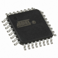
AT89LP828-20MH Atmel, AT89LP828-20MH Datasheet - Page 10

AT89LP828-20MH
Manufacturer Part Number
AT89LP828-20MH
Description
MCU 8051 8K FLASH SPI 32VQFN
Manufacturer
Atmel
Series
89LPr
Datasheet
1.AT89LP428-20AU.pdf
(149 pages)
Specifications of AT89LP828-20MH
Core Processor
8051
Core Size
8-Bit
Speed
20MHz
Connectivity
SPI, UART/USART
Peripherals
Brown-out Detect/Reset, POR, PWM, WDT
Number Of I /o
30
Program Memory Size
8KB (8K x 8)
Program Memory Type
FLASH
Eeprom Size
1K x 8
Ram Size
768 x 8
Voltage - Supply (vcc/vdd)
2.4 V ~ 5.5 V
Oscillator Type
Internal
Operating Temperature
-40°C ~ 85°C
Package / Case
32-TQFP
Lead Free Status / RoHS Status
Lead free / RoHS Compliant
Data Converters
-
Available stocks
Company
Part Number
Manufacturer
Quantity
Price
Company:
Part Number:
AT89LP828-20MH
Manufacturer:
Atmel
Quantity:
720
- Current page: 10 of 149
- Download datasheet (5Mb)
3.2
3.2.1
3.2.2
3.2.3
10
Internal Data Memory
AT89LP428/828
DATA
IDATA
SFR
In order to read from the signature arrays, the SIGEN bit (DPCF.3) must be set. While SIGEN is
one, MOVC A,@A+DPTR will access the signature arrays. The User Signature Array is mapped
from addresses 0080H to 00FFH and the Atmel Signature Array is mapped from addresses
0000H to 003FH. SIGEN must be cleared before using MOVC to access the code memory. The
User Signature Array may also be modified by the In-Application Programming interface. When
IAP = 1 and SIGEN = 1, MOVX @DPTR instructions will access the array.
The AT89LP428/828 contains 256 bytes of general SRAM data memory plus 128 bytes of I/O
memory mapped into a single 8-bit address space. Access to the internal data memory does not
require any configuration. The internal data memory has three address spaces: DATA, IDATA
and SFR; as shown in
Figure 3-2.
The first 128 bytes of RAM are directly addressable by an 8-bit address (00H - 7FH) included in
the instruction. The lowest 32 bytes of DATA memory are grouped into 4 banks of 8 registers
each. The RS0 and RS1 bits (PSW.3 and PSW.4) select which register bank is in use. Instruc-
tions using register addressing will only access the currently specified bank.
The full 256 bytes of internal RAM can be indirectly addressed using the 8-bit pointers R0 and
R1. The first 128 bytes of IDATA include the DATA space. The hardware stack is also located in
the IDATA space.
The upper 128 direct addresses (80H - FFH) access the I/O registers. I/O registers on AT89LP
devices are referred to as Special Function Registers. The SFRs can only be accessed through
direct addressing. All SFR locations are not implemented.
page 15.
Lower
Upper
128
128
FFH
7F H
80H
0
Internal Data Memory Map
Indirect Addressing
DATA/IDATA
by Direct and
Accessible
Addressing
Accessible
Figure
by Indirect
IDATA
Only
Only
3-2.
Addressing
Accessible
by Direct
SFR
Special
Function
Registers
See “Special Function Registers” on
FFH
80H
Status and Control Bits
Ports
Timers
Registers
Stack Pointer
Accumulator
(Etc.)
3654A–MICRO–8/09
Related parts for AT89LP828-20MH
Image
Part Number
Description
Manufacturer
Datasheet
Request
R

Part Number:
Description:
Manufacturer:
Atmel Corporation
Datasheet:

Part Number:
Description:
MCU 8051 8K FLASH SPI 32TQFP
Manufacturer:
Atmel
Datasheet:

Part Number:
Description:
MCU 8051 8K FLASH SPI 32PLCC
Manufacturer:
Atmel
Datasheet:

Part Number:
Description:
MCU 8051 8K FLASH SPI 28PDIP
Manufacturer:
Atmel
Datasheet:

Part Number:
Description:
IC MCU 8051 8KB FLASH 28PDIP
Manufacturer:
Atmel
Datasheet:

Part Number:
Description:
IC MCU 8051 8KB FLASH 32PLCC
Manufacturer:
Atmel
Datasheet:

Part Number:
Description:
8-bit Microcontrollers - MCU Single-Cycle 8051 8K ISP Flash, 2.4-5.5V
Manufacturer:
Atmel
Datasheet:

Part Number:
Description:
DEV KIT FOR AVR/AVR32
Manufacturer:
Atmel
Datasheet:

Part Number:
Description:
INTERVAL AND WIPE/WASH WIPER CONTROL IC WITH DELAY
Manufacturer:
ATMEL Corporation
Datasheet:

Part Number:
Description:
Low-Voltage Voice-Switched IC for Hands-Free Operation
Manufacturer:
ATMEL Corporation
Datasheet:

Part Number:
Description:
MONOLITHIC INTEGRATED FEATUREPHONE CIRCUIT
Manufacturer:
ATMEL Corporation
Datasheet:

Part Number:
Description:
AM-FM Receiver IC U4255BM-M
Manufacturer:
ATMEL Corporation
Datasheet:

Part Number:
Description:
Monolithic Integrated Feature Phone Circuit
Manufacturer:
ATMEL Corporation
Datasheet:

Part Number:
Description:
Multistandard Video-IF and Quasi Parallel Sound Processing
Manufacturer:
ATMEL Corporation
Datasheet:


