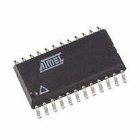
AT90PWM2-16SQ Atmel, AT90PWM2-16SQ Datasheet - Page 186
AT90PWM2-16SQ
Manufacturer Part Number
AT90PWM2-16SQ
Description
IC AVR MCU FLASH 8K 24SOIC
Manufacturer
Atmel
Series
AVR® 90PWM Lightingr
Datasheet
1.AT90PWM3B-16SU.pdf
(361 pages)
Specifications of AT90PWM2-16SQ
Core Processor
AVR
Core Size
8-Bit
Speed
16MHz
Connectivity
SPI, UART/USART
Peripherals
Brown-out Detect/Reset, POR, PWM, WDT
Number Of I /o
19
Program Memory Size
8KB (8K x 8)
Program Memory Type
FLASH
Eeprom Size
512 x 8
Ram Size
512 x 8
Voltage - Supply (vcc/vdd)
2.7 V ~ 5.5 V
Data Converters
A/D 8x10b; D/A 1x10b
Oscillator Type
Internal
Operating Temperature
-40°C ~ 105°C
Package / Case
24-SOIC (7.5mm Width)
Processor Series
AT90PWMx
Core
AVR8
Data Bus Width
8 bit
Data Ram Size
512 B
Interface Type
SPI, USART
Maximum Clock Frequency
16 MHz
Number Of Programmable I/os
19
Number Of Timers
2
Operating Supply Voltage
2.7 V to 5.5 V
Maximum Operating Temperature
+ 105 C
Mounting Style
SMD/SMT
3rd Party Development Tools
EWAVR, EWAVR-BL
Development Tools By Supplier
ATAVRDRAGON, ATSTK500, ATSTK600, ATAVRISP2, ATAVRONEKIT, ATAVRFBKIT, ATAVRISP2
Minimum Operating Temperature
- 40 C
On-chip Adc
10 bit, 8 Channel
On-chip Dac
10 bit, 1 Channel
For Use With
ATSTK600-SOIC - STK600 SOCKET/ADAPTER FOR SOICATAVRFBKIT - KIT DEMO BALLAST FOR AT90PWM2ATSTK520 - ADAPTER KIT FOR 90PWM
Lead Free Status / RoHS Status
Lead free / RoHS Compliant


18.3.2
18.3.3
186
AT90PWM2/3/2B/3B
Double Speed Operation (U2X)
External Clock
Table 18-1
ing the UBRR value for each mode of operation using an internally generated clock source.
Table 18-1.
Note:
Some examples of UBRR values for some system clock frequencies are found in
(see
The transfer rate can be doubled by setting the U2X bit in UCSRA. Setting this bit only has effect
for the asynchronous operation. Set this bit to zero when using synchronous operation.
Setting this bit will reduce the divisor of the baud rate divider from 16 to 8, effectively doubling
the transfer rate for asynchronous communication. Note however that the Receiver will in this
case only use half the number of samples (reduced from 16 to 8) for data sampling and clock
recovery, and therefore a more accurate baud rate setting and system clock are required when
this mode is used. For the Transmitter, there are no downsides.
External clocking is used by the synchronous slave modes of operation. The description in this
section refers to
External clock input from the XCK pin is sampled by a synchronization register to minimize the
chance of meta-stability. The output from the synchronization register must then pass through
an edge detector before it can be used by the Transmitter and Receiver. This process intro-
duces a two CPU clock period delay and therefore the maximum external XCK clock frequency
is limited by the following equation:
Operating Mode
Asynchronous Normal mode
(U2X = 0)
Asynchronous Double Speed
mode (U2X = 1)
Synchronous Master mode
BAUD Baud rate (in bits per second, bps).
f
UBRR Contents of the UBRRH and UBRRL Registers, (0-4095).
clk
page
io
1. The baud rate is defined to be the transfer rate in bit per second (bps)
System I/O Clock frequency.
207).
contains equations for calculating the baud rate (in bits per second) and for calculat-
Equations for Calculating Baud Rate Register Setting
Figure 18-2
for details.
Equation for Calculating Baud
BAUD
BAUD
BAUD
=
=
=
----------------------------------------- -
16 UBRRn
Rate
-------------------------------------- -
8 UBRRn
-------------------------------------- -
2 UBRRn
f
XCKn
(
(
(
(1)
f
f
f
CLKio
CLKio
CLKio
<
f
--------------- -
CLKio
4
+
+
+
1
1
1
)
)
)
Equation for Calculating UBRR
UBRRn
UBRRn
UBRRn
=
Value
=
=
----------------------- - 1
16BAUD
------------------- - 1
8BAUD
------------------- - 1
2BAUD
f
f
f
CLKio
CLKio
CLKio
4317J–AVR–08/10
Table 18-9
–
–
–
Related parts for AT90PWM2-16SQ
Image
Part Number
Description
Manufacturer
Datasheet
Request
R

Part Number:
Description:
At90pwm2 8-bit Avr Microcontroller With 8k Bytes In-system Programmable Flash
Manufacturer:
ATMEL Corporation
Datasheet:


Part Number:
Description:
DEV KIT FOR AVR/AVR32
Manufacturer:
Atmel
Datasheet:
Part Number:
Description:
INTERVAL AND WIPE/WASH WIPER CONTROL IC WITH DELAY
Manufacturer:
ATMEL Corporation
Datasheet:
Part Number:
Description:
Low-Voltage Voice-Switched IC for Hands-Free Operation
Manufacturer:
ATMEL Corporation
Datasheet:
Part Number:
Description:
MONOLITHIC INTEGRATED FEATUREPHONE CIRCUIT
Manufacturer:
ATMEL Corporation
Datasheet:
Part Number:
Description:
AM-FM Receiver IC U4255BM-M
Manufacturer:
ATMEL Corporation
Datasheet:
Part Number:
Description:
Monolithic Integrated Feature Phone Circuit
Manufacturer:
ATMEL Corporation
Datasheet:
Part Number:
Description:
Multistandard Video-IF and Quasi Parallel Sound Processing
Manufacturer:
ATMEL Corporation
Datasheet:
Part Number:
Description:
High-performance EE PLD
Manufacturer:
ATMEL Corporation
Datasheet:
Part Number:
Description:
8-bit Flash Microcontroller
Manufacturer:
ATMEL Corporation
Datasheet:
Part Number:
Description:
2-Wire Serial EEPROM
Manufacturer:
ATMEL Corporation
Datasheet: