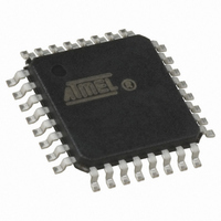
AT90USB162-16AUR Atmel, AT90USB162-16AUR Datasheet - Page 224

AT90USB162-16AUR
Manufacturer Part Number
AT90USB162-16AUR
Description
IC AVR MCU 16K FLASH 32TQFP
Manufacturer
Atmel
Series
AVR® 90USBr
Datasheet
1.AT90USB82-16MU.pdf
(307 pages)
Specifications of AT90USB162-16AUR
Core Processor
AVR
Core Size
8-Bit
Speed
16MHz
Connectivity
EBI/EMI, PS/2, SPI, UART/USART, USB
Peripherals
Brown-out Detect/Reset, POR, PWM, WDT
Number Of I /o
22
Program Memory Size
16KB (16K x 8)
Program Memory Type
FLASH
Eeprom Size
512 x 8
Ram Size
512 x 8
Voltage - Supply (vcc/vdd)
2.7 V ~ 5.5 V
Oscillator Type
Internal
Operating Temperature
-40°C ~ 85°C
Package / Case
32-TQFP, 32-VQFP
Processor Series
AT90USBx
Core
AVR8
Data Bus Width
8 bit
Data Ram Size
512 B
Interface Type
SPI/USART/debugWIRE
Maximum Clock Frequency
16 MHz
Number Of Programmable I/os
22
Number Of Timers
2
Operating Supply Voltage
2.7 V to 5.5 V
Maximum Operating Temperature
+ 85 C
Mounting Style
SMD/SMT
3rd Party Development Tools
EWAVR, EWAVR-BL
Development Tools By Supplier
ATAVRDRAGON, ATSTK500, ATSTK600, ATSTK525, ATSTK526, ATAVRISP2, ATAVRONEKIT, AT90USBKEY, ATEVK525
Minimum Operating Temperature
- 40 C
Cpu Family
AT90
Device Core
AVR
Device Core Size
8b
Frequency (max)
16MHz
Total Internal Ram Size
512Byte
# I/os (max)
22
Number Of Timers - General Purpose
2
Operating Supply Voltage (typ)
3.3/5V
Operating Supply Voltage (max)
5.5V
Operating Supply Voltage (min)
2.7V
Instruction Set Architecture
RISC
Operating Temp Range
-40C to 85C
Operating Temperature Classification
Industrial
Mounting
Surface Mount
Pin Count
32
Package Type
TQFP
For Use With
ATSTK600-TQFP32 - STK600 SOCKET/ADAPTER 32-TQFPATSTK526 - KIT STARTER FOR AT90USB82/162ATAVRDRAGON - KIT DRAGON 32KB FLASH MEM AVRATSTK525 - KIT STARTER FOR AT90USBAT90USBKEY2 - KIT DEMO FOR AT90USB
Lead Free Status / RoHS Status
Lead free / RoHS Compliant
Data Converters
-
Lead Free Status / Rohs Status
Lead free / RoHS Compliant
Other names
AT90USB162-16AU
AT90USB162-16AURTR
AT90USB162-16AUTR
AT90USB162-16AUTR
AT90USB162-16AURTR
AT90USB162-16AUTR
AT90USB162-16AUTR
Available stocks
Company
Part Number
Manufacturer
Quantity
Price
Company:
Part Number:
AT90USB162-16AUR
Manufacturer:
Atmel
Quantity:
2 751
- Current page: 224 of 307
- Download datasheet (4Mb)
22.0.2
224
AT90USB82/162
Digital Input Disable Register 1 – DIDR1
• Bit 4 – ACI: Analog Comparator Interrupt Flag
This bit is set by hardware when a comparator output event triggers the interrupt mode defined
by ACIS1 and ACIS0. The Analog Comparator interrupt routine is executed if the ACIE bit is set
and the I-bit in SREG is set. ACI is cleared by hardware when executing the corresponding inter-
rupt handling vector. Alternatively, ACI is cleared by writing a logic one to the flag.
• Bit 3 – ACIE: Analog Comparator Interrupt Enable
When the ACIE bit is written logic one and the I-bit in the Status Register is set, the Analog Com-
parator interrupt is activated. When written logic zero, the interrupt is disabled.
• Bit 2 – ACIC: Analog Comparator Input Capture Enable
When written logic one, this bit enables the input capture function in Timer/Counter1 to be trig-
gered by the Analog Comparator. The comparator output is in this case directly connected to the
input capture front-end logic, making the comparator utilize the noise canceler and edge select
features of the Timer/Counter1 Input Capture interrupt. When written logic zero, no connection
between the Analog Comparator and the input capture function exists. To make the comparator
trigger the Timer/Counter1 Input Capture interrupt, the ICIE1 bit in the Timer Interrupt Mask
Register (TIMSK1) must be set.
• Bits 1, 0 – ACIS1, ACIS0: Analog Comparator Interrupt Mode Select
These bits determine which comparator events that trigger the Analog Comparator interrupt. The
different settings are shown in
Table 22-1.
When changing the ACIS1/ACIS0 bits, the Analog Comparator Interrupt must be disabled by
clearing its Interrupt Enable bit in the ACSR Register. Otherwise an interrupt can occur when the
bits are changed.
• Bit 1, 0 – AIN1D, AIN0D: AIN1, AIN0 Digital Input Disable
When this bit is written logic one, the digital input buffer on the AIN1/0 pin is disabled. The corre-
sponding PIN Register bit will always read as zero when this bit is set. When an analog signal is
applied to the AIN1/0 pin and the digital input from this pin is not needed, this bit should be writ-
ten logic one to reduce power consumption in the digital input buffer.
Bit
Read/Write
Initial Value
ACIS1
0
0
1
1
ACIS1/ACIS0 Settings
7
–
R
0
ACIS0
0
1
0
1
6
–
R
0
Interrupt Mode
Comparator Interrupt on Output Toggle.
Reserved
Comparator Interrupt on Falling Output Edge.
Comparator Interrupt on Rising Output Edge.
Table
5
–
R
0
22-1.
4
–
R
0
3
–
R
0
2
–
R
0
1
AIN1D
R/W
0
0
AIN0D
R/W
0
7707F–AVR–11/10
DIDR1
Related parts for AT90USB162-16AUR
Image
Part Number
Description
Manufacturer
Datasheet
Request
R

Part Number:
Description:
Manufacturer:
Atmel Corporation
Datasheet:

Part Number:
Description:
MCU AVR USB 16K FLASH 32-TQFP
Manufacturer:
Atmel
Datasheet:

Part Number:
Description:
MCU AVR USB 16K FLASH 32-QFN
Manufacturer:
Atmel
Datasheet:

Part Number:
Description:
IC AVR MCU 16K FLASH 32QFN
Manufacturer:
Atmel
Datasheet:

Part Number:
Description:
MCU, MPU & DSP Development Tools PROTOTYPE BRD FOR AT90USB162
Manufacturer:
Olimex Ltd.
Datasheet:

Part Number:
Description:
MCU, MPU & DSP Development Tools DEV BRD FOR AT90USB162
Manufacturer:
Olimex Ltd.
Datasheet:

Part Number:
Description:
MCU, MPU & DSP Development Tools Demo board f/AVR MCU & AT90USB
Manufacturer:
Atmel
Datasheet:

Part Number:
Description:
DEV KIT FOR AVR/AVR32
Manufacturer:
Atmel
Datasheet:

Part Number:
Description:
INTERVAL AND WIPE/WASH WIPER CONTROL IC WITH DELAY
Manufacturer:
ATMEL Corporation
Datasheet:

Part Number:
Description:
Low-Voltage Voice-Switched IC for Hands-Free Operation
Manufacturer:
ATMEL Corporation
Datasheet:

Part Number:
Description:
MONOLITHIC INTEGRATED FEATUREPHONE CIRCUIT
Manufacturer:
ATMEL Corporation
Datasheet:

Part Number:
Description:
AM-FM Receiver IC U4255BM-M
Manufacturer:
ATMEL Corporation
Datasheet:

Part Number:
Description:
Monolithic Integrated Feature Phone Circuit
Manufacturer:
ATMEL Corporation
Datasheet:

Part Number:
Description:
Multistandard Video-IF and Quasi Parallel Sound Processing
Manufacturer:
ATMEL Corporation
Datasheet:


