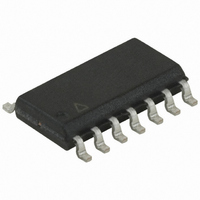
ATTINY84V-10SSU Atmel, ATTINY84V-10SSU Datasheet - Page 126

ATTINY84V-10SSU
Manufacturer Part Number
ATTINY84V-10SSU
Description
MCU AVR 8K ISP FLASH 1.8V 14SOIC
Manufacturer
Atmel
Series
AVR® ATtinyr
Specifications of ATTINY84V-10SSU
Core Processor
AVR
Core Size
8-Bit
Speed
10MHz
Connectivity
USI
Peripherals
Brown-out Detect/Reset, POR, PWM, Temp Sensor, WDT
Number Of I /o
12
Program Memory Size
8KB (4K x 16)
Program Memory Type
FLASH
Eeprom Size
512 x 8
Ram Size
512 x 8
Voltage - Supply (vcc/vdd)
1.8 V ~ 5.5 V
Data Converters
A/D 8x10b
Oscillator Type
Internal
Operating Temperature
-40°C ~ 85°C
Package / Case
14-SOIC (3.9mm Width), 14-SOL
Processor Series
ATTINY8x
Core
AVR8
Data Bus Width
8 bit
Data Ram Size
512 B
Interface Type
SPI
Maximum Clock Frequency
10 MHz
Number Of Programmable I/os
12
Number Of Timers
2
Maximum Operating Temperature
+ 85 C
Mounting Style
SMD/SMT
Minimum Operating Temperature
- 40 C
On-chip Adc
10 bit, 8 Channel
Package
14SOIC
Device Core
AVR
Family Name
ATtiny
Maximum Speed
10 MHz
Operating Supply Voltage
2.5|3.3|5 V
For Use With
ATSTK600 - DEV KIT FOR AVR/AVR32770-1007 - ISP 4PORT ATMEL AVR MCU SPI/JTAG770-1004 - ISP 4PORT FOR ATMEL AVR MCU SPIATAVRISP2 - PROGRAMMER AVR IN SYSTEM
Lead Free Status / RoHS Status
Lead free / RoHS Compliant
- Current page: 126 of 238
- Download datasheet (5Mb)
14.5.4
126
ATtiny24/44/84
USICR – USI Control Register
The 4-bit counter increments by one for each clock generated either by the external clock edge
detector, by a Timer/Counter0 Compare Match, or by software using USICLK or USITC strobe
bits. The clock source depends on the setting of the USICS1:0 bits.
For external clock operation a special feature is added that allows the clock to be generated by
writing to the USITC strobe bit. This feature is enabled by choosing an external clock source
(USICS1 = 1) and writing a one to the USICLK bit.
Note that even when no wire mode is selected (USIWM1:0 = 0) the external clock input
(USCK/SCL) can still be used by the counter.
The USI Control Register includes bits for interrupt enable, setting the wire mode, selecting the
clock and clock strobe.
• Bit 7 – USISIE: Start Condition Interrupt Enable
Setting this bit to one enables the start condition detector interrupt. If there is a pending interrupt
and USISIE and the Global Interrupt Enable Flag are set to one the interrupt will be executed
immediately. Refer to the USISIF bit description on
• Bit 6 – USIOIE: Counter Overflow Interrupt Enable
Setting this bit to one enables the counter overflow interrupt. If there is a pending interrupt and
USIOIE and the Global Interrupt Enable Flag are set to one the interrupt will be executed imme-
diately. Refer to the USIOIF bit description on
• Bits 5:4 – USIWM1, USIWM0: Wire Mode
These bits set the type of wire mode to be used, as shown in
Basically, only the function of the outputs are affected by these bits. Data and clock inputs are
not affected by the mode selected and will always have the same function. The counter and USI
Data Register can therefore be clocked externally and data input sampled, even when outputs
are disabled.
Bit
0x0D (0x2D)
Read/Write
Initial Value
USISIE
R/W
7
0
USIOIE
R/W
6
0
USIWM1
R/W
5
0
USIWM0
R/W
4
0
page 125
page 125
USICS1
R/W
3
0
for further details.
Table 14-1 on page
for further details.
USICS0
R/W
2
0
USICLK
W
1
0
USITC
127.
8006K–AVR–10/10
W
0
0
USICR
Related parts for ATTINY84V-10SSU
Image
Part Number
Description
Manufacturer
Datasheet
Request
R

Part Number:
Description:
IC MCU AVR 8K FLASH 10MHZ 20-QFN
Manufacturer:
Atmel
Datasheet:

Part Number:
Description:
MCU AVR 8KB FLASH 10MHZ 14SOIC
Manufacturer:
Atmel
Datasheet:

Part Number:
Description:
MCU AVR 8KB FLASH 10MHZ 20QFN
Manufacturer:
Atmel
Datasheet:

Part Number:
Description:
AVR MCU, 8K FLASH, 512B RAM, 512B EE
Manufacturer:
Atmel
Datasheet:

Part Number:
Description:
Manufacturer:
Atmel Corporation
Datasheet:

Part Number:
Description:
Manufacturer:
Atmel Corporation
Datasheet:

Part Number:
Description:
IC MCU AVR 8K FLASH 20MHZ 20-QFN
Manufacturer:
Atmel
Datasheet:

Part Number:
Description:
MCU AVR 8K ISP FLASH 2.7V 14SOIC
Manufacturer:
Atmel
Datasheet:

Part Number:
Description:
MCU AVR 8K FLASH 15MHZ 20-QFN
Manufacturer:
Atmel
Datasheet:

Part Number:
Description:
IC MCU AVR 8K FLASH 20MHZ 14-DIP
Manufacturer:
Atmel
Datasheet:

Part Number:
Description:
MCU AVR 8KB FLASH 10MHZ 14SOIC
Manufacturer:
Atmel
Datasheet:

Part Number:
Description:
MCU AVR 8KB FLASH 20MHZ 20QFN
Manufacturer:
Atmel
Datasheet:

Part Number:
Description:
IC, MCU, 8BIT, 2K FLASH, 20SOIC
Manufacturer:
Atmel
Datasheet:

Part Number:
Description:
IC, MCU, 8BIT, 2K FLASH, 20PDIP
Manufacturer:
Atmel
Datasheet:

Part Number:
Description:
IC, MCU, 8BIT, 8K FLASH, 20PDIP
Manufacturer:
Atmel
Datasheet:


