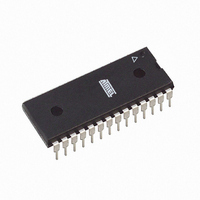
ATMEGA8A-PU Atmel, ATMEGA8A-PU Datasheet - Page 61

ATMEGA8A-PU
Manufacturer Part Number
ATMEGA8A-PU
Description
MCU AVR 8K FLASH 16MHZ 28-PDIP
Manufacturer
Atmel
Series
AVR® ATmegar
Specifications of ATMEGA8A-PU
Core Processor
AVR
Core Size
8-Bit
Speed
16MHz
Connectivity
I²C, SPI, UART/USART
Peripherals
Brown-out Detect/Reset, POR, PWM, WDT
Number Of I /o
23
Program Memory Size
8KB (4K x 16)
Program Memory Type
FLASH
Eeprom Size
512 x 8
Ram Size
1K x 8
Voltage - Supply (vcc/vdd)
2.7 V ~ 5.5 V
Data Converters
A/D 6x10b
Oscillator Type
Internal
Operating Temperature
-40°C ~ 85°C
Package / Case
28-DIP (0.300", 7.62mm)
Processor Series
ATMEGA8x
Core
AVR8
Data Bus Width
8 bit
Data Ram Size
1 KB
Interface Type
SPI, TWI, USART
Maximum Clock Frequency
16 MHz
Number Of Programmable I/os
23
Number Of Timers
3
Maximum Operating Temperature
+ 85 C
Mounting Style
Through Hole
3rd Party Development Tools
EWAVR, EWAVR-BL
Development Tools By Supplier
ATAVRDRAGON, ATSTK500, ATSTK600, ATAVRISP2, ATAVRONEKIT
Minimum Operating Temperature
- 40 C
On-chip Adc
10 bit, 6 Channel
Package
28PDIP
Device Core
AVR
Family Name
ATmega
Maximum Speed
16 MHz
Operating Supply Voltage
3.3|5 V
Controller Family/series
AVR MEGA
No. Of I/o's
23
Eeprom Memory Size
512Byte
Ram Memory Size
1KB
Cpu Speed
16MHz
Rohs Compliant
Yes
For Use With
ATSTK600 - DEV KIT FOR AVR/AVR32ATSTK500 - PROGRAMMER AVR STARTER KIT
Lead Free Status / RoHS Status
Lead free / RoHS Compliant
Available stocks
Company
Part Number
Manufacturer
Quantity
Price
Part Number:
ATMEGA8A-PU
Manufacturer:
ATMEL/爱特梅尔
Quantity:
20 000
- Current page: 61 of 308
- Download datasheet (6Mb)
12.3.3
8159D–AVR–02/11
Alternate Functions of Port C
The Port C pins with alternate functions are shown in
Table 12-5.
The alternate pin configuration is as follows:
• RESET – Port C, Bit 6
RESET, Reset pin: When the RSTDISBL Fuse is programmed, this pin functions as a normal I/O
pin, and the part will have to rely on Power-on Reset and Brown-out Reset as its reset sources.
When the RSTDISBL Fuse is unprogrammed, the reset circuitry is connected to the pin, and the
pin can not be used as an I/O pin.
If PC6 is used as a reset pin, DDC6, PORTC6 and PINC6 will all read 0.
• SCL/ADC5 – Port C, Bit 5
SCL, Two-wire Serial Interface Clock: When the TWEN bit in TWCR is set (one) to enable the
Two-wire Serial Interface, pin PC5 is disconnected from the port and becomes the Serial Clock
I/O pin for the Two-wire Serial Interface. In this mode, there is a spike filter on the pin to sup-
press spikes shorter than 50 ns on the input signal, and the pin is driven by an open drain driver
with slew-rate limitation.
PC5 can also be used as ADC input Channel 5. Note that ADC input channel 5 uses digital
power.
• SDA/ADC4 – Port C, Bit 4
SDA, Two-wire Serial Interface Data: When the TWEN bit in TWCR is set (one) to enable the
Two-wire Serial Interface, pin PC4 is disconnected from the port and becomes the Serial Data
I/O pin for the Two-wire Serial Interface. In this mode, there is a spike filter on the pin to sup-
press spikes shorter than 50 ns on the input signal, and the pin is driven by an open drain driver
with slew-rate limitation.
PC4 can also be used as ADC input Channel 4. Note that ADC input channel 4 uses digital
power.
• ADC3 – Port C, Bit 3
PC3 can also be used as ADC input Channel 3. Note that ADC input channel 3 uses analog
power.
Port Pin
PC6
PC5
PC4
PC3
PC2
PC1
PC0
Port C Pins Alternate Functions
Alternate Function
RESET (Reset pin)
ADC5 (ADC Input Channel 5)
SCL (Two-wire Serial Bus Clock Line)
ADC4 (ADC Input Channel 4)
SDA (Two-wire Serial Bus Data Input/Output Line)
ADC3 (ADC Input Channel 3)
ADC2 (ADC Input Channel 2)
ADC1 (ADC Input Channel 1)
ADC0 (ADC Input Channel 0)
Table
12-5.
ATmega8A
61
Related parts for ATMEGA8A-PU
Image
Part Number
Description
Manufacturer
Datasheet
Request
R

Part Number:
Description:
IC AVR MCU 8K 16MHZ 5V 32TQFP
Manufacturer:
Atmel
Datasheet:

Part Number:
Description:
IC AVR MCU 8K 16MHZ 5V 32-QFN
Manufacturer:
Atmel
Datasheet:

Part Number:
Description:
IC AVR MCU 8K 16MHZ 5V 28DIP
Manufacturer:
Atmel
Datasheet:

Part Number:
Description:
IC AVR MCU 8K 16MHZ COM 32-TQFP
Manufacturer:
Atmel
Datasheet:

Part Number:
Description:
IC AVR MCU 8K 16MHZ IND 32-TQFP
Manufacturer:
Atmel
Datasheet:

Part Number:
Description:
IC AVR MCU 8K 16MHZ COM 28-DIP
Manufacturer:
Atmel
Datasheet:

Part Number:
Description:
IC AVR MCU 8K 16MHZ IND 28-DIP
Manufacturer:
Atmel
Datasheet:

Part Number:
Description:
IC AVR MCU 8K 16MHZ COM 32-QFN
Manufacturer:
Atmel
Datasheet:

Part Number:
Description:
MCU AVR 8KB FLASH 16MHZ 32QFN
Manufacturer:
Atmel
Datasheet:

Part Number:
Description:
IC AVR MCU 8K 16MHZ IND 32-QFN
Manufacturer:
Atmel
Datasheet:

Part Number:
Description:
IC MCU AVR 8K 5V 16MHZ 32-TQFP
Manufacturer:
Atmel
Datasheet:

Part Number:
Description:
IC MCU AVR 8K 5V 16MHZ 32-QFN
Manufacturer:
Atmel
Datasheet:

Part Number:
Description:
IC MCU AVR 8K 5V 16MHZ 28-DIP
Manufacturer:
Atmel
Datasheet:


