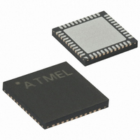
ATMEGA162-16MUR Atmel, ATMEGA162-16MUR Datasheet - Page 27

ATMEGA162-16MUR
Manufacturer Part Number
ATMEGA162-16MUR
Description
MCU AVR 16KB FLASH 16MHZ 44QFN
Manufacturer
Atmel
Series
AVR® ATmegar
Specifications of ATMEGA162-16MUR
Core Processor
AVR
Core Size
8-Bit
Speed
16MHz
Connectivity
EBI/EMI, SPI, UART/USART
Peripherals
Brown-out Detect/Reset, POR, PWM, WDT
Number Of I /o
35
Program Memory Size
16KB (8K x 16)
Program Memory Type
FLASH
Eeprom Size
512 x 8
Ram Size
1K x 8
Voltage - Supply (vcc/vdd)
2.7 V ~ 5.5 V
Oscillator Type
Internal
Operating Temperature
-40°C ~ 85°C
Package / Case
44-VQFN Exposed Pad
For Use With
ATSTK600-TQFP44 - STK600 SOCKET/ADAPTER 44-TQFPATSTK500 - PROGRAMMER AVR STARTER KIT
Lead Free Status / RoHS Status
Lead free / RoHS Compliant
Data Converters
-
- Current page: 27 of 324
- Download datasheet (6Mb)
Address Latch
Requirements
2513K–AVR–07/09
The control bits for the External Memory Interface are located in three registers, the MCU Con-
trol Register – MCUCR, the Extended MCU Control Register – EMCUCR, and the Special
Function IO Register – SFIOR.
When the XMEM interface is enabled, it will override the settings in the Data Direction registers
corresponding to the ports dedicated to the interface. For details about this port override, see the
alternate functions in section
whether an access is internal or external. If the access is external, the XMEM interface will out-
put address, data, and the control signals on the ports according to
the wave forms without wait-states). When ALE goes from high to low, there is a valid address
on AD7:0. ALE is low during a data transfer. When the XMEM interface is enabled, also an inter-
nal access will cause activity on address-, data- and ALE ports, but the RD and WR strobes will
not toggle during internal access. When the External Memory Interface is disabled, the normal
pin and data direction settings are used. Note that when the XMEM interface is disabled, the
address space above the internal SRAM boundary is not mapped into the internal SRAM.
12
“74x573” or equivalent) which is transparent when G is high.
Due to the high-speed operation of the XRAM interface, the address latch must be selected with
care for system frequencies above 8 MHz @ 4V and 4 MHz @ 2.7V. When operating at condi-
tions above these frequencies, the typical old style 74HC series latch becomes inadequate. The
external memory interface is designed in compliance to the 74AHC series latch. However, most
latches can be used as long they comply with the main timing parameters. The main parameters
for the address latch are:
•
•
•
The external memory interface is designed to guaranty minimum address hold time after G is
asserted low of t
D to Q propagation delay (t
requirement of the external component. The data setup time before G low (t
address valid to ALE low (t
Figure 12. External SRAM Connected to the AVR
illustrates how to connect an external SRAM to the AVR using an octal latch (typically
D to Q propagation delay (t
Data setup time before G low (t
Data (address) hold time after G low (
h
= 5 ns (refer to t
AVR
AD7:0
A15:8
AVLLC
pd
ALE
WR
RD
) must be taken into consideration when calculating the access time
pd
“I/O-Ports” on page
) minus PCB wiring delay (dependent on the capacitive load).
).
LAXX_LD
su
).
/t
th
LLAXX_ST
).
D
G
in
Q
Table 114
63. The XMEM interface will autodetect
to
D[7:0]
A[15:8]
A[7:0]
RD
WR
SRAM
Table 121 on page
Figure 13
ATmega162/V
su
) must not exceed
(this figure shows
272). The
Figure
27
Related parts for ATMEGA162-16MUR
Image
Part Number
Description
Manufacturer
Datasheet
Request
R

Part Number:
Description:
Manufacturer:
Atmel Corporation
Datasheet:

Part Number:
Description:
IC AVR MCU 16K 16MHZ 5V 44TQFP
Manufacturer:
Atmel
Datasheet:

Part Number:
Description:
IC AVR MCU 16K 16MHZ 5V 40DIP
Manufacturer:
Atmel
Datasheet:

Part Number:
Description:
IC AVR MCU 16K 16MHZ 5V 44-QFN
Manufacturer:
Atmel
Datasheet:

Part Number:
Description:
IC MCU AVR 16K 5V 16MHZ 44-TQFP
Manufacturer:
Atmel
Datasheet:

Part Number:
Description:
IC MCU AVR 16K 5V 16MHZ 44-QFN
Manufacturer:
Atmel
Datasheet:

Part Number:
Description:
MCU AVR 16KB FLASH 16MHZ 44TQFP
Manufacturer:
Atmel
Datasheet:

Part Number:
Description:
IC MCU AVR 16K 5V 16MHZ 44-TQFP
Manufacturer:
Atmel
Datasheet:

Part Number:
Description:
IC MCU AVR 16K 5V 16MHZ 44-QFN
Manufacturer:
Atmel
Datasheet:

Part Number:
Description:
IC MCU AVR 16K 5V 16MHZ 40-DIP
Manufacturer:
Atmel
Datasheet:

Part Number:
Description:
IC MCU AVR 16K 5V 16MHZ 40-DIP
Manufacturer:
Atmel
Datasheet:

Part Number:
Description:
IC MCU AVR 16K 5V 16MHZ 44-TQFP
Manufacturer:
Atmel
Datasheet:

Part Number:
Description:
IC MCU AVR 16K 5V 16MHZ 44-QFN
Manufacturer:
Atmel
Datasheet:


