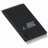
ATMEGA16HVA-4TU Atmel, ATMEGA16HVA-4TU Datasheet - Page 152

ATMEGA16HVA-4TU
Manufacturer Part Number
ATMEGA16HVA-4TU
Description
MCU AVR 16K FLASH 4MHZ 28-TSOP
Manufacturer
Atmel
Series
AVR® ATmegar
Datasheet
1.ATMEGA16HVA-4CKU.pdf
(196 pages)
Specifications of ATMEGA16HVA-4TU
Core Processor
AVR
Core Size
8-Bit
Speed
4MHz
Connectivity
SPI
Peripherals
Brown-out Detect/Reset, POR, PWM, WDT
Number Of I /o
7
Program Memory Size
16KB (8K x 16)
Program Memory Type
FLASH
Eeprom Size
256 x 8
Ram Size
512 x 8
Voltage - Supply (vcc/vdd)
1.8 V ~ 9 V
Data Converters
A/D 5x12b
Oscillator Type
External
Operating Temperature
-20°C ~ 85°C
Package / Case
28-TSOP
For Use With
ATSTK600 - DEV KIT FOR AVR/AVR32ATSTK500 - PROGRAMMER AVR STARTER KIT
Lead Free Status / RoHS Status
Lead free / RoHS Compliant
Available stocks
Company
Part Number
Manufacturer
Quantity
Price
Company:
Part Number:
ATMEGA16HVA-4TU
Manufacturer:
Atmel
Quantity:
20
- Current page: 152 of 196
- Download datasheet (3Mb)
27.6.1
152
ATmega8HVA/16HVA
Serial Programming Algorithm
Figure 27-1. Serial Programming and Verify.
Table 27-8.
When programming the EEPROM, an auto-erase cycle is built into the self-timed programming
operation (in the Serial mode ONLY) and there is no need to first execute the Chip Erase
instruction. The Chip Erase operation turns the content of every memory location in both the
Program and EEPROM arrays into 0xFF.
Depending on OSCSEL Fuses, a valid clock must be present. The minimum low and high peri-
ods for the serial clock (SCK) input are defined as follows:
Low: > 2.2 CPU clock cycles for f
High: > 2.2 CPU clock cycles for f
When writing serial data to the ATmega8HVA/16HVA, data is clocked on the rising edge of SCK.
When reading data from the ATmega8HVA/16HVA, data is clocked on the falling edge of SCK.
See
To program and verify the ATmega8HVA/16HVA in the Serial Programming mode, the following
sequence is recommended (see four byte instruction formats in
1. Power-up sequence:
2. Wait for at least 20 ms and enable serial programming by sending the Programming
Apply power between V
tems, the programmer can not guarantee that SCK is held low during power-up. In this
case, RESET must be given a positive pulse of at least two CPU clock cycles duration
after SCK has been set to “0”.
Enable serial instruction to pin MOSI.
”Serial Programming” on page 172
Symbol
MOSI
MISO
SCK
Pin Mapping Serial Programming
MOSI
MISO
SCK
CC
and GND while RESET and SCK are set to “0”. In some sys-
Pins
PB1
PB2
PB3
ck
ck
< 12 MHz, 3 CPU clock cycles for f
< 12 MHz, 3 CPU clock cycles for f
RESET
GND
for timing details.
I/O
O
I
I
VCC
+3.0 - 4.5V
Table 27-10 on page
Serial Data out
Serial Data in
Description
Serial Clock
ck
ck
>= 12 MHz
>= 12 MHz
8024A–AVR–04/08
154):
Related parts for ATMEGA16HVA-4TU
Image
Part Number
Description
Manufacturer
Datasheet
Request
R

Part Number:
Description:
Manufacturer:
Atmel Corporation
Datasheet:

Part Number:
Description:
IC AVR MCU 16K 16MHZ 5V 44TQFP
Manufacturer:
Atmel
Datasheet:

Part Number:
Description:
IC AVR MCU 16K 16MHZ 5V 44-QFN
Manufacturer:
Atmel
Datasheet:

Part Number:
Description:
IC AVR MCU 16K 16MHZ 5V 40DIP
Manufacturer:
Atmel
Datasheet:

Part Number:
Description:
MCU AVR 16K FLASH 16MHZ 44-QFN
Manufacturer:
Atmel
Datasheet:

Part Number:
Description:
IC AVR MCU 16K 16MHZ COM 40-DIP
Manufacturer:
Atmel
Datasheet:

Part Number:
Description:
IC AVR MCU 16K 16MHZ COM 44-QFN
Manufacturer:
Atmel
Datasheet:

Part Number:
Description:
IC AVR MCU 16K 16MHZ IND 40-DIP
Manufacturer:
Atmel
Datasheet:

Part Number:
Description:
IC AVR MCU 16K 16MHZ IND 44-QFN
Manufacturer:
Atmel
Datasheet:

Part Number:
Description:
IC AVR MCU 16K 16MHZ IND 44-TQFP
Manufacturer:
Atmel
Datasheet:

Part Number:
Description:
IC MCU 8BIT 16KB FLASH 44TQFP
Manufacturer:
Atmel
Datasheet:

Part Number:
Description:
MCU AVR 16K FLASH 16MHZ 44-TQFP
Manufacturer:
Atmel
Datasheet:

Part Number:
Description:
IC AVR MCU 16K 16MHZ COM 44-TQFP
Manufacturer:
Atmel
Datasheet:


