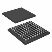
ATXMEGA64A1-C7U Atmel, ATXMEGA64A1-C7U Datasheet - Page 11

ATXMEGA64A1-C7U
Manufacturer Part Number
ATXMEGA64A1-C7U
Description
IC MCU AVR 64KB FLASH 100VFBGA
Manufacturer
Atmel
Series
AVR® XMEGAr
Datasheet
1.ATAVRONEKIT.pdf
(113 pages)
Specifications of ATXMEGA64A1-C7U
Core Processor
AVR
Core Size
8/16-Bit
Speed
32MHz
Connectivity
EBI/EMI, I²C, IrDA, SPI, UART/USART
Peripherals
Brown-out Detect/Reset, DMA, POR, PWM, WDT
Number Of I /o
78
Program Memory Size
64KB (32K x 16)
Program Memory Type
FLASH
Eeprom Size
2K x 8
Ram Size
4K x 8
Voltage - Supply (vcc/vdd)
1.6 V ~ 3.6 V
Data Converters
A/D 16x12b, D/A 4x12b
Oscillator Type
Internal
Operating Temperature
-40°C ~ 85°C
Package / Case
100-VFBGA
Processor Series
XMEGA
Core
AVR
Data Bus Width
8 bit, 16 bit
Data Ram Size
4 KB
Interface Type
SPI, TWI, USART
Maximum Clock Frequency
32 MHz
Number Of Programmable I/os
78
Number Of Timers
8
Operating Supply Voltage
2.5 V
Maximum Operating Temperature
+ 85 C
Mounting Style
SMD/SMT
3rd Party Development Tools
EWAVR, EWAVR-BL
Development Tools By Supplier
ATAVRDRAGON, ATAVRISP2, ATAVRONEKIT
Minimum Operating Temperature
- 40 C
Operating Temperature Range
- 40 C to + 85 C
Lead Free Status / RoHS Status
Lead free / RoHS Compliant
Available stocks
Company
Part Number
Manufacturer
Quantity
Price
7.3
7.4
Figure 7-2.
8067M–AVR–09/10
Byte Address
In-System Programmable Flash Program Memory
Data Memory
17FF
1000
FFF
Data Memory Map (Hexadecimal address)
0
ATxmega192A1
I/O Registers
RESERVED
EEPROM
(4 KB)
(2 KB)
The XMEGA A1 devices contain On-chip In-System Programmable Flash memory for program
storage, see
Flash address location is 16 bits.
The Program Flash memory space is divided into Application and Boot sections. Both sections
have dedicated Lock Bits for setting restrictions on write or read/write operations. The Store Pro-
gram Memory (SPM) instruction must reside in the Boot Section when used to write to the Flash
memory.
A third section inside the Application section is referred to as the Application Table section which
has separate Lock bits for storage of write or read/write protection. The Application Table sec-
tion can be used for storing non-volatile data or application software.
Figure 7-1.
The Application Table Section and Boot Section can also be used for general application
software.
The Data Memory consists of the I/O Memory, EEPROM and SRAM memories, all within one
linear address space, see
all devices in the family is identical and with empty, reserved memory space for smaller devices.
2EFFF
2FFFF
30FFF
2F000
30000
/
/
/
/
/
Figure 7-1 on page
Flash Program Memory (Hexadecimal address)
1EFFF
1FFFF
20FFF
1F000
20000
Byte Address
Word Address
/
/
/
/
/
Figure 7-2 on page
17FF
1000
FFF
16FFF
17FFF
18FFF
17000
18000
0
11. Since all AVR instructions are 16- or 32-bits wide, each
ATxmega128A1
/
/
/
/
/
I/O Registers
RESERVED
EEPROM
10FFF
(4 KB)
(2 KB)
10000
EFFF
FFFF
F000
11. To simplify development, the memory map for
/
/
/
/
/
7FFF
77FF
87FF
7800
8000
0
Byte Address
Application Table Section (Bytes)
(384K/256K/192K/128K/64K)
Application Section (Bytes)
Boot Section (Bytes)
(8K/8K/8K/8K/4K)
(8K/8K/8K/8K/4K)
17FF
1000
FFF
0
XMEGA A1
...
ATxmega64A1
I/O Registers
RESERVED
EEPROM
(4 KB)
(2 KB)
11


