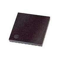
ATMEGA168-15MZ Atmel, ATMEGA168-15MZ Datasheet - Page 154

ATMEGA168-15MZ
Manufacturer Part Number
ATMEGA168-15MZ
Description
MCU AVR 16K FLASH 15MHZ 32-QFN
Manufacturer
Atmel
Series
AVR® ATmegar
Datasheet
1.ATMEGA168-15MZ.pdf
(340 pages)
Specifications of ATMEGA168-15MZ
Package / Case
32-VQFN Exposed Pad, 32-HVQFN, 32-SQFN, 32-DHVQFN
Voltage - Supply (vcc/vdd)
2.7 V ~ 5.5 V
Operating Temperature
-40°C ~ 125°C
Speed
16MHz
Number Of I /o
23
Eeprom Size
512 x 8
Core Processor
AVR
Program Memory Type
FLASH
Ram Size
1K x 8
Program Memory Size
16KB (16K x 8)
Data Converters
A/D 8x10b
Oscillator Type
Internal
Peripherals
Brown-out Detect/Reset, POR, PWM, WDT
Connectivity
I²C, SPI, UART/USART
Core Size
8-Bit
Processor Series
ATMEGA16x
Core
AVR8
Data Bus Width
8 bit
Data Ram Size
1 KB
Interface Type
2-Wire, SPI, USART, Serial
Maximum Clock Frequency
20 MHz
Number Of Programmable I/os
23
Number Of Timers
3
Maximum Operating Temperature
+ 85 C
Mounting Style
SMD/SMT
3rd Party Development Tools
EWAVR, EWAVR-BL
Development Tools By Supplier
ATAVRDRAGON, ATSTK500, ATSTK600, ATAVRISP2, ATAVRONEKIT
Minimum Operating Temperature
- 40 C
On-chip Adc
10 bit, 8 Channel
Package
32QFN EP
Device Core
AVR
Family Name
ATmega
Maximum Speed
16 MHz
Operating Supply Voltage
3.3|5 V
Lead Free Status / RoHS Status
Lead free / RoHS Compliant
Available stocks
Company
Part Number
Manufacturer
Quantity
Price
Company:
Part Number:
ATMEGA168-15MZ
Manufacturer:
ATMEL
Quantity:
1 300
Part Number:
ATMEGA168-15MZ
Manufacturer:
ATMEL/爱特梅尔
Quantity:
20 000
- Current page: 154 of 340
- Download datasheet (6Mb)
15.9.2
154
ATmega48/88/168 Automotive
Asynchronous Status Register – ASSR
• Bit 6 – EXCLK: Enable External Clock Input
When EXCLK is written to one, and asynchronous clock is selected, the external clock input buf-
fer is enabled and an external clock can be input on Timer Oscillator 1 (TOSC1) pin instead of a
32 kHz crystal. Writing to EXCLK should be done before asynchronous operation is selected.
Note that the crystal Oscillator will only run when this bit is zero.
• Bit 5 – AS2: Asynchronous Timer/Counter2
When AS2 is written to zero, Timer/Counter2 is clocked from the I/O clock, clk
written to one, Timer/Counter2 is clocked from a crystal Oscillator connected to the Timer Oscil-
lator 1 (TOSC1) pin. When the value of AS2 is changed, the contents of TCNT2, OCR2A,
OCR2B, TCCR2A and TCCR2B might be corrupted.
• Bit 4 – TCN2UB: Timer/Counter2 Update Busy
When Timer/Counter2 operates asynchronously and TCNT2 is written, this bit becomes set.
When TCNT2 has been updated from the temporary storage register, this bit is cleared by hard-
ware. A logical zero in this bit indicates that TCNT2 is ready to be updated with a new value.
• Bit 3 – OCR2AUB: Output Compare Register2 Update Busy
When Timer/Counter2 operates asynchronously and OCR2A is written, this bit becomes set.
When OCR2A has been updated from the temporary storage register, this bit is cleared by hard-
ware. A logical zero in this bit indicates that OCR2A is ready to be updated with a new value.
• Bit 2 – OCR2BUB: Output Compare Register2 Update Busy
When Timer/Counter2 operates asynchronously and OCR2B is written, this bit becomes set.
When OCR2B has been updated from the temporary storage register, this bit is cleared by hard-
ware. A logical zero in this bit indicates that OCR2B is ready to be updated with a new value.
• Bit 1 – TCR2AUB: Timer/Counter Control Register2 Update Busy
When Timer/Counter2 operates asynchronously and TCCR2A is written, this bit becomes set.
When TCCR2A has been updated from the temporary storage register, this bit is cleared by
hardware. A logical zero in this bit indicates that TCCR2A is ready to be updated with a new
value.
• Bit 0 – TCR2BUB: Timer/Counter Control Register2 Update Busy
When Timer/Counter2 operates asynchronously and TCCR2B is written, this bit becomes set.
When TCCR2B has been updated from the temporary storage register, this bit is cleared by
hardware. A logical zero in this bit indicates that TCCR2B is ready to be updated with a new
value.
If a write is performed to any of the five Timer/Counter2 Registers while its update busy flag is
set, the updated value might get corrupted and cause an unintentional interrupt to occur.
The mechanisms for reading TCNT2, OCR2A, OCR2B, TCCR2A and TCCR2B are different.
When reading TCNT2, the actual timer value is read. When reading OCR2A, OCR2B, TCCR2A
and TCCR2B the value in the temporary storage register is read.
Bit
Read/Write
Initial Value
R
7
–
0
EXCLK
R/W
6
0
AS2
R/W
5
0
TCN2UB
R
4
0
OCR2AUB
R
3
0
OCR2BUB
R
2
0
TCR2AUB
R
1
0
TCR2BUB
I/O
. When AS2 is
R
0
0
7530I–AVR–02/10
ASSR
Related parts for ATMEGA168-15MZ
Image
Part Number
Description
Manufacturer
Datasheet
Request
R

Part Number:
Description:
Manufacturer:
Atmel Corporation
Datasheet:

Part Number:
Description:
Manufacturer:
Atmel Corporation
Datasheet:

Part Number:
Description:
Manufacturer:
ATMEL Corporation
Datasheet:

Part Number:
Description:
IC AVR MCU 16K 20MHZ 32TQFP
Manufacturer:
Atmel
Datasheet:

Part Number:
Description:
IC AVR MCU 16K 20MHZ 32-QFN
Manufacturer:
Atmel
Datasheet:

Part Number:
Description:
IC AVR MCU 16K 20MHZ 28DIP
Manufacturer:
Atmel
Datasheet:

Part Number:
Description:
MCU AVR 16K FLASH 15MHZ 32-TQFP
Manufacturer:
Atmel
Datasheet:

Part Number:
Description:
IC AVR MCU 16K 20MHZ 32TQFP
Manufacturer:
Atmel
Datasheet:

Part Number:
Description:
MCU AVR 16KB FLASH 20MHZ 32QFN
Manufacturer:
Atmel
Datasheet:

Part Number:
Description:
MCU AVR 16KB FLASH 20MHZ 32TQFP
Manufacturer:
Atmel
Datasheet:

Part Number:
Description:
IC MCU AVR 16K FLASH 32-QFN
Manufacturer:
Atmel
Datasheet:


