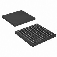
AT91SAM7SE32-CU-999 Atmel, AT91SAM7SE32-CU-999 Datasheet - Page 23

AT91SAM7SE32-CU-999
Manufacturer Part Number
AT91SAM7SE32-CU-999
Description
IC MCU ARM7 32KB FLASH 144LFBGA
Manufacturer
Atmel
Series
AT91SAMr
Datasheet
1.AT91SAM7SE32-CU-999.pdf
(47 pages)
Specifications of AT91SAM7SE32-CU-999
Core Processor
ARM7
Core Size
16/32-Bit
Speed
55MHz
Connectivity
EBI/EMI, I²C, SPI, SSC, UART/USART, USB
Peripherals
Brown-out Detect/Reset, POR, PWM, WDT
Number Of I /o
88
Program Memory Size
32KB (32K x 8)
Program Memory Type
FLASH
Ram Size
8K x 8
Voltage - Supply (vcc/vdd)
1.65 V ~ 1.95 V
Data Converters
A/D 8x10b
Oscillator Type
Internal
Operating Temperature
-40°C ~ 85°C
Package / Case
144-LFBGA
Processor Series
AT91SAMx
Core
ARM7TDMI
Data Bus Width
32 bit
Data Ram Size
8 KB
Interface Type
EBI, SPI, TWI, USART
Maximum Clock Frequency
55 MHz
Number Of Programmable I/os
88
Number Of Timers
3
Maximum Operating Temperature
+ 85 C
Mounting Style
SMD/SMT
3rd Party Development Tools
JTRACE-ARM-2M, KSK-AT91SAM7S-PL, MDK-ARM, RL-ARM, ULINK2
Development Tools By Supplier
AT91SAM-ICE, AT91-ISP, AT91SAM7SE-EK
Minimum Operating Temperature
- 40 C
On-chip Adc
10 bit, 8 Channel
For Use With
AT91SAM7SE-EK - EVAL BOARD FOR AT91SAM7SEAT91SAM-ICE - EMULATOR FOR AT91 ARM7/ARM9
Lead Free Status / RoHS Status
Lead free / RoHS Compliant
Eeprom Size
-
Lead Free Status / Rohs Status
Details
Available stocks
Company
Part Number
Manufacturer
Quantity
Price
8.1
8.1.1
8.1.1.1
8.1.1.2
8.1.1.3
6222ES–ATARM–15-Dec-09
Embedded Memories
Internal Memories
Internal SRAM
Internal ROM
Internal Flash
A first level of address decoding is performed by the Memory Controller, i.e., by the implementa-
tion of the Advanced System Bus (ASB) with additional features.
Decoding splits the 4G bytes of address space into 16 areas of 256M bytes. The areas 1 to 8 are
directed to the EBI that associates these areas to the external chip selects NC0 to NCS7. The
area 0 is reserved for the addressing of the internal memories, and a second level of decoding
provides 1M byte of internal memory area. The area 15 is reserved for the peripherals and pro-
vides access to the Advanced Peripheral Bus (APB).
Other areas are unused and performing an access within them provides an abort to the master
requesting such an access.
The AT91SAM7SE512/256 embeds a high-speed 32-Kbyte SRAM bank. The AT91SAM7SE32
embeds a high-speed 8-Kbyte SRAM bank. After reset and until the Remap Command is per-
formed, the SRAM is only accessible at address 0x0020 0000. After Remap, the SRAM also
becomes available at address 0x0.
The AT91SAM7SE512/256/32 embeds an Internal ROM. At any time, the ROM is mapped at
address 0x30 0000. The ROM contains the FFPI and the SAM-BA boot program.
At any time, the Flash is mapped to address 0x0010 0000.
A general purpose NVM (GPNVM) bit is used to boot either on the ROM (default) or from the
Flash.
This GPNVM bit can be cleared or set respectively through the commands “Clear General-pur-
pose NVM Bit” and “Set General-purpose NVM Bit” of the EFC User Interface.
Setting the GPNVM bit 2 selects the boot from the Flash, clearing it selects the boot from the
ROM. Asserting ERASE clears the GPNVM bit 2 and thus selects the boot from the ROM by
default.
• The AT91SAM7SE512 features two banks of 256 Kbytes of Flash.
• The AT91SAM7SE256 features one bank of 256 Kbytes of Flash.
• The AT91SAM7SE32 features one bank of 32 Kbytes of Flash.
AT91SAM7SE512/256/32 Preliminary Summary
23


