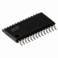
P89LPC931A1FDH,512 NXP Semiconductors, P89LPC931A1FDH,512 Datasheet - Page 21

P89LPC931A1FDH,512
Manufacturer Part Number
P89LPC931A1FDH,512
Description
IC 80C51 MCU FLASH 8K 28-TSSOP
Manufacturer
NXP Semiconductors
Series
LPC900r
Datasheet
1.P89LPC9301FDH512.pdf
(66 pages)
Specifications of P89LPC931A1FDH,512
Program Memory Type
FLASH
Program Memory Size
8KB (8K x 8)
Package / Case
28-TSSOP
Core Processor
8051
Core Size
8-Bit
Speed
18MHz
Connectivity
I²C, SPI, UART/USART
Peripherals
Brown-out Detect/Reset, POR, PWM, WDT
Number Of I /o
26
Ram Size
256 x 8
Voltage - Supply (vcc/vdd)
2.4 V ~ 3.6 V
Oscillator Type
Internal
Operating Temperature
-40°C ~ 85°C
Processor Series
P89LPC
Core
80C51
Data Bus Width
8 bit
Data Ram Size
256 B
Interface Type
I2C, SPI, UART
Maximum Clock Frequency
18 MHz
Number Of Programmable I/os
23
Number Of Timers
3
Operating Supply Voltage
2.4 V to 3.6 V
Maximum Operating Temperature
+ 85 C
Mounting Style
SMD/SMT
3rd Party Development Tools
PK51, CA51, A51, ULINK2
Minimum Operating Temperature
- 40 C
Lead Free Status / RoHS Status
Lead free / RoHS Compliant
For Use With
568-1758 - BOARD EVAL FOR LPC93X MCU FAMILY
Eeprom Size
-
Data Converters
-
Lead Free Status / Rohs Status
Lead free / RoHS Compliant
Other names
935288634512
NXP Semiconductors
P89LPC9301_931A1
Product data sheet
7.13 Memory organization
7.14 Data RAM arrangement
7.15 Interrupts
The various P89LPC9301/931A1 memory spaces are as follows:
The 256 bytes of on-chip RAM are organized as shown in
Table 6.
The P89LPC9301/931A1 uses a four priority level interrupt structure. This allows great
flexibility in controlling the handling of the many interrupt sources. The
P89LPC9301/931A1 supports 13 interrupt sources: external interrupts 0 and 1, timers 0
and 1, serial port TX, serial port RX, combined serial port RX/TX, brownout detect,
watchdog/RTC, I
Each interrupt source can be individually enabled or disabled by setting or clearing a bit in
the interrupt enable registers IEN0 or IEN1. The IEN0 register also contains a global
disable bit, EA, which disables all interrupts.
Each interrupt source can be individually programmed to one of four priority levels by
setting or clearing bits in the interrupt priority registers IP0, IP0H, IP1 and IP1H. An
interrupt service routine in progress can be interrupted by a higher priority interrupt, but
not by another interrupt of the same or lower priority. The highest priority interrupt service
cannot be interrupted by any other interrupt source. If two requests of different priority
levels are pending at the start of an instruction, the request of higher priority level is
serviced.
Type
DATA
IDATA
•
•
•
•
DATA
128 bytes of internal data memory space (00H:7FH) accessed via direct or indirect
addressing, using instructions other than MOVX and MOVC. All or part of the Stack
may be in this area.
IDATA
Indirect Data. 256 bytes of internal data memory space (00H:FFH) accessed via
indirect addressing using instructions other than MOVX and MOVC. All or part of the
Stack may be in this area. This area includes the DATA area and the 128 bytes
immediately above it.
SFR
Special Function Registers. Selected CPU registers and peripheral control and status
registers, accessible only via direct addressing.
CODE
64 kB of Code memory space, accessed as part of program execution and via the
MOVC instruction. The P89LPC9301/931A1 has 4 kB/8 kB of on-chip Code memory.
On-chip data memory usages
Data RAM
Memory that can be addressed directly and indirectly
Memory that can be addressed indirectly
All information provided in this document is subject to legal disclaimers.
2
C-bus, keyboard, comparators 1 and 2, SPI.
Rev. 2 — 29 November 2010
8-bit microcontroller with accelerated two-clock 80C51 core
P89LPC9301/931A1
Table
6.
© NXP B.V. 2010. All rights reserved.
Size (bytes)
128
256
21 of 66


