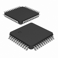
P87C51RB2BBD,157 NXP Semiconductors, P87C51RB2BBD,157 Datasheet - Page 11

P87C51RB2BBD,157
Manufacturer Part Number
P87C51RB2BBD,157
Description
IC 80C51 MCU 512 RAM 44LQFP
Manufacturer
NXP Semiconductors
Series
87Cr
Datasheet
1.P87C51RC2FA512.pdf
(67 pages)
Specifications of P87C51RB2BBD,157
Program Memory Type
OTP
Program Memory Size
16KB (16K x 8)
Package / Case
44-LQFP
Core Processor
8051
Core Size
8-Bit
Speed
33MHz
Connectivity
EBI/EMI, UART/USART
Peripherals
POR, PWM, WDT
Number Of I /o
32
Ram Size
512 x 8
Voltage - Supply (vcc/vdd)
2.7 V ~ 5.5 V
Oscillator Type
Internal
Operating Temperature
0°C ~ 70°C
Processor Series
P87C5x
Core
80C51
Data Bus Width
8 bit
Data Ram Size
512 B
Interface Type
UART
Maximum Clock Frequency
33 MHz
Number Of Programmable I/os
32
Number Of Timers
3
Operating Supply Voltage
2.7 V to 5.5 V
Maximum Operating Temperature
+ 70 C
Mounting Style
SMD/SMT
3rd Party Development Tools
PK51, CA51, A51, ULINK2
Minimum Operating Temperature
0 C
Lead Free Status / RoHS Status
Lead free / RoHS Compliant
For Use With
OM10064 - EMULATOR 80C51 PDS51-MK2
Eeprom Size
-
Data Converters
-
Lead Free Status / Rohs Status
Lead free / RoHS Compliant
Other names
935271877157
P87C51RB2BBD
P87C51RB2BBD
P87C51RB2BBD
P87C51RB2BBD
Available stocks
Company
Part Number
Manufacturer
Quantity
Price
Company:
Part Number:
P87C51RB2BBD,157
Manufacturer:
NXP Semiconductors
Quantity:
10 000
Philips Semiconductors
CLOCK CONTROL REGISTER (CKCON)
This device allows control of the 6-clock/12-clock mode by means of
both an SFR bit (X2) and an OTP bit. The OTP clock control bit
Also please note that the clock divider applies to the serial port for
modes 0 & 2 (fixed baud rate modes). This is because modes 1 & 3
(variable baud rate modes) use either Timer 1 or Timer 2.
Below is the truth table for the CPU clock mode.
Table 1.
2003 Jan 24
OX2 clock mode bit
(can only be set by
parallel programmer)
erased
erased
programmed
80C51 8-bit microcontroller family
with 512B/1KB RAM, low voltage (2.7 to 5.5 V), low power, high
speed (30/33 MHz)
CKCON
BIT
CKCON.7
CKCON.6
CKCON.5
CKCON.4
CKCON.3
CKCON.2
CKCON.1
CKCON.0
Not Bit Addressable
Address = 8Fh
SYMBOL
–
X2
X2 bit
(CKCON.0)
0
1
X
FUNCTION
Reserved.
Reserved.
Reserved.
Reserved.
Reserved.
Reserved.
Reserved.
CPU clock; 1 = 6 clocks for each machine cycle, 0 = 12 clocks for each machine cycle
–
7
8KB/16KB/32KB/64KB OTP
CPU clock mode
12-clock mode
(default)
6-clock mode
6-clock mode
–
6
Figure 1. Clock control (CKCON) register
–
5
4
–
11
3
–
OX2, when programmed (6-clock mode), supersedes the X2 bit
(CKCON.0). The CKCON register is shown below in Figure 1.
RESET
A reset is accomplished by holding the RST pin high for at least two
machine cycles (12 oscillator periods in 6-clock mode, or 24 oscillator
periods in 12-clock mode), while the oscillator is running. To ensure a
good power-on reset, the RST pin must be high long enough to allow
the oscillator time to start up (normally a few milliseconds) plus two
machine cycles. At power-on, the voltage on V
come up at the same time for a proper start-up. Ports 1, 2, and 3 will
asynchronously be driven to their reset condition when a voltage
above V
The value on the EA pin is latched when RST is deasserted and has
no further effect.
IH1
2
–
(min.) is applied to RST.
P87C51RA2/RB2/RC2/RD2
1
–
0
X2
Reset Value = x0000000B
CC
and RST must
SU01689
Product data


