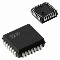
P89LPC932A1FA,112 NXP Semiconductors, P89LPC932A1FA,112 Datasheet - Page 19

P89LPC932A1FA,112
Manufacturer Part Number
P89LPC932A1FA,112
Description
IC 80C51 MCU FLASH 8K 28-PLCC
Manufacturer
NXP Semiconductors
Series
LPC900r
Datasheet
1.P89LPC932A1FDH529.pdf
(64 pages)
Specifications of P89LPC932A1FA,112
Core Processor
8051
Core Size
8-Bit
Speed
18MHz
Connectivity
I²C, SPI, UART/USART
Peripherals
Brown-out Detect/Reset, LED, POR, PWM, WDT
Number Of I /o
26
Program Memory Size
8KB (8K x 8)
Program Memory Type
FLASH
Ram Size
768 x 8
Voltage - Supply (vcc/vdd)
2.4 V ~ 3.6 V
Oscillator Type
Internal
Operating Temperature
-40°C ~ 85°C
Package / Case
28-PLCC
Processor Series
P89LPC9x
Core
80C51
Data Bus Width
8 bit
Data Ram Size
768 B
Interface Type
I2C, SPI, UART
Maximum Clock Frequency
12 MHz
Number Of Programmable I/os
26
Number Of Timers
2
Operating Supply Voltage
2.4 V to 3.6 V
Maximum Operating Temperature
+ 85 C
Mounting Style
SMD/SMT
3rd Party Development Tools
PK51, CA51, A51, ULINK2
Minimum Operating Temperature
- 40 C
For Use With
OM6292 - DEMO BOARD PCA2125 RTCDB-TSSOP-LPC932 - BOARD FOR LPC932 TSSOP622-1014 - BOARD FOR LPC9XX TSSOP622-1008 - BOARD FOR LPC9103 10-HVSON622-1006 - SOCKET ADAPTER BOARDMCB900K - BOARD PROTOTYPE NXP 89LPC9EPM900K - EMULATOR/PROGRAMMER NXP P89LPC9568-4000 - DEMO BOARD SPI/I2C TO DUAL UART568-3510 - DEMO BOARD SPI/I2C TO UART622-1003 - KIT FOR LCD DEMO622-1002 - USB IN-CIRCUIT PROG LPC9XX568-1759 - EMULATOR DEBUGGER/PROGRMMR LPC9X568-1758 - BOARD EVAL FOR LPC93X MCU FAMILY
Lead Free Status / RoHS Status
Lead free / RoHS Compliant
Eeprom Size
-
Data Converters
-
Lead Free Status / Rohs Status
Details
Other names
568-4279-5
935276131112
P89LPC932A1FA
935276131112
P89LPC932A1FA
Available stocks
Company
Part Number
Manufacturer
Quantity
Price
Company:
Part Number:
P89LPC932A1FA,112
Manufacturer:
NXP Semiconductors
Quantity:
10 000
NXP Semiconductors
P89LPC932A1_3
Product data sheet
7.10 Memory organization
7.7 CCLK wake-up delay
7.8 CCLK modification: DIVM register
7.9 Low power select
The P89LPC932A1 has an internal wake-up timer that delays the clock until it stabilizes
depending on the clock source used. If the clock source is any of the three crystal
selections (low, medium and high frequencies) the delay is 992 OSCCLK cycles plus
60 s to 100 s. If the clock source is either the internal RC oscillator, watchdog oscillator,
or external clock, the delay is 224 OSCCLK cycles plus 60 s to 100 s.
The OSCCLK frequency can be divided down up to 510 times by configuring a dividing
register, DIVM, to generate CCLK. This feature makes it possible to temporarily run the
CPU at a lower rate, reducing power consumption. By dividing the clock, the CPU can
retain the ability to respond to events that would not exit Idle mode by executing its normal
program at a lower rate. This can also allow bypassing the oscillator start-up time in cases
where Power-down mode would otherwise be used. The value of DIVM may be changed
by the program at any time without interrupting code execution.
The P89LPC932A1 is designed to run at 12 MHz (CCLK) maximum. However, if CCLK is
8 MHz or slower, the CLKLP SFR bit (AUXR1.7) can be set to logic 1 to lower the power
consumption further. On any reset, CLKLP is logic 0 allowing highest performance
access. This bit can then be set in software if CCLK is running at 8 MHz or slower.
The various P89LPC932A1 memory spaces are as follows:
•
•
•
•
DATA
128 bytes of internal data memory space (00H:7FH) accessed via direct or indirect
addressing, using instructions other than MOVX and MOVC. All or part of the Stack
may be in this area.
IDATA
Indirect Data. 256 bytes of internal data memory space (00H:FFH) accessed via
indirect addressing using instructions other than MOVX and MOVC. All or part of the
Stack may be in this area. This area includes the DATA area and the 128 bytes
immediately above it.
SFR
Special Function Registers. Selected CPU registers and peripheral control and status
registers, accessible only via direct addressing.
XDATA
‘External’ Data or Auxiliary RAM. Duplicates the classic 80C51 64 kB memory space
addressed via the MOVX instruction using the SPTR, R0, or R1. All or part of this
space could be implemented on-chip. The P89LPC932A1 has 512 bytes of on-chip
XDATA memory.
Rev. 03 — 12 March 2007
8-bit microcontroller with accelerated two-clock 80C51 core
P89LPC932A1
© NXP B.V. 2007. All rights reserved.
19 of 64


