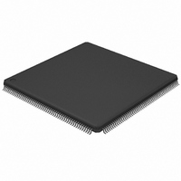
LPC2420FBD208,551 NXP Semiconductors, LPC2420FBD208,551 Datasheet - Page 24

LPC2420FBD208,551
Manufacturer Part Number
LPC2420FBD208,551
Description
IC ARM7 MCU ROMLESS 208LQFP
Manufacturer
NXP Semiconductors
Series
LPC2400r
Datasheet
1.LPC2460FBD208551.pdf
(79 pages)
Specifications of LPC2420FBD208,551
Program Memory Type
ROMless
Package / Case
208-LQFP
Core Processor
ARM7
Core Size
16/32-Bit
Speed
72MHz
Connectivity
EBI/EMI, I²C, Microwire, MMC, SPI, SSI, SSP, UART/USART, USB OTG
Peripherals
Brown-out Detect/Reset, DMA, I²S, POR, PWM, WDT
Number Of I /o
160
Ram Size
82K x 8
Voltage - Supply (vcc/vdd)
3 V ~ 3.6 V
Data Converters
A/D 8x10b; D/A 1x10b
Oscillator Type
Internal
Operating Temperature
-40°C ~ 85°C
Processor Series
LPC24
Core
ARM7TDMI-S
Data Bus Width
16 bit, 32 bit
Data Ram Size
82 KB
Interface Type
CAN/I2C/I2S/SPI/SSP/UART/USB
Maximum Clock Frequency
72 MHz
Number Of Programmable I/os
160
Number Of Timers
4
Operating Supply Voltage
3.3 V
Maximum Operating Temperature
+ 85 C
Mounting Style
SMD/SMT
3rd Party Development Tools
MDK-ARM, RL-ARM, ULINK2
Minimum Operating Temperature
- 40 C
On-chip Adc
8-ch x 10-bit
On-chip Dac
1-ch x 10-bit
Lead Free Status / RoHS Status
Lead free / RoHS Compliant
Eeprom Size
-
Program Memory Size
-
Lead Free Status / Rohs Status
Lead free / RoHS Compliant
Other names
568-4527
935286745551
935286745551
Available stocks
Company
Part Number
Manufacturer
Quantity
Price
Company:
Part Number:
LPC2420FBD208,551
Manufacturer:
NXP Semiconductors
Quantity:
10 000
NXP Semiconductors
Table 4.
[1]
[2]
[3]
[4]
[5]
[6]
[7]
[8]
LPC2420_60_5
Preliminary data sheet
Symbol
V
V
V
V
n.c.
V
V
VREF
VBAT
SSIO
SSCORE
SSA
DD(3V3)
DD(DCDC)(3V3)
DDA
5 V tolerant pad providing digital I/O functions with TTL levels and hysteresis.
5 V tolerant pad providing digital I/O functions (with TTL levels and hysteresis) and analog input. When configured as a ADC input,
digital section of the pad is disabled.
5 V tolerant pad providing digital I/O with TTL levels and hysteresis and analog output function. When configured as the DAC output,
digital section of the pad is disabled.
Open-drain 5 V tolerant digital I/O pad, compatible with I
functionality. When power is switched off, this pin connected to the I
configuration applies to all functions on this pin.
Pad provides digital I/O and USB functions. It is designed in accordance with the USB specification, revision 2.0 (Full-speed and
Low-speed mode only).
5 V tolerant pad with 5 ns glitch filter providing digital I/O functions with TTL levels and hysteresis.
5 V tolerant pad with 20 ns glitch filter providing digital I/O function with TTL levels and hysteresis.
Pad provides special analog functionality.
Pin description
Pin
33, 63,
77, 93,
114,
133,
148,
169,
189,
200
32, 84,
172
22
15, 60,
71, 89,
112,
125,
146,
165,
181,
198
30, 117,
141
26, 86,
174
20
24
38
[8]
[8]
[8]
[8]
[8]
[8]
[8]
[8]
[8]
…continued
Ball
L3, T5,
R9,
P12,
N16,
H14,
E15,
A12,
B6, A2
K4, P10,
D12
J2
G3,
P6, P8,
U13,
P17,
K16,
C17,
B13,
C9,
D7
J4, L14,
G14
H4, P11,
D11
G4
K1
M3
[8]
[8]
[8]
[8]
[8]
[8]
[8]
[8]
[8]
Type
I
I
I
I
I
I
I
I
I
Rev. 05 — 24 February 2010
Description
ground: 0 V reference for the digital I/O pins.
ground: 0 V reference for the core.
analog ground: 0 V reference. This should nominally be the same
voltage as V
error.
3.3 V supply voltage: This is the power supply voltage for the I/O ports.
not connected pins: These pins must be left unconnected (floating).
3.3 V DC-to-DC converter supply voltage: This is the power supply for
the on-chip DC-to-DC converter.
analog 3.3 V pad supply voltage: This should be nominally the same
voltage as V
This voltage is used to power the ADC and DAC.
ADC reference: This should be nominally the same voltage as V
but should be isolated to minimize noise and error. The level on this pin is
used as a reference for ADC and DAC.
RTC power supply: 3.3 V on this pin supplies the power to the RTC.
2
C-bus 400 kHz specification. It requires an external pull-up to provide output
SSIO
DD(3V3)
2
C-bus is floating and does not disturb the I
/V
SSCORE
but should be isolated to minimize noise and error.
, but should be isolated to minimize noise and
Flashless 16-bit/32-bit microcontroller
LPC2420/2460
2
C-bus lines. Open-drain
© NXP B.V. 2010. All rights reserved.
DD(3V3)
24 of 79


