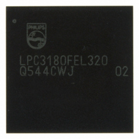
LPC3180FEL320 NXP Semiconductors, LPC3180FEL320 Datasheet - Page 17

LPC3180FEL320
Manufacturer Part Number
LPC3180FEL320
Description
IC ARM9 MCU 208MHZ 320-LFBGA
Manufacturer
NXP Semiconductors
Series
LPC3000r
Datasheet
1.LPC3180FEL320.pdf
(36 pages)
Specifications of LPC3180FEL320
Core Size
16/32-Bit
Oscillator Type
External
Core Processor
ARM9
Speed
208MHz
Connectivity
EBI/EMI, I²C, MMC, SPI, UART/USART, USB OTG
Peripherals
DMA, PWM, WDT
Number Of I /o
55
Program Memory Type
ROMless
Ram Size
64K x 8
Voltage - Supply (vcc/vdd)
1.1 V ~ 3.3 V
Data Converters
A/D 3x10b
Operating Temperature
-40°C ~ 85°C
Package / Case
320-LFBGA
No. Of I/o's
55
Ram Memory Size
64KB
Cpu Speed
208MHz
No. Of Timers
1
No. Of Pwm Channels
2
Digital Ic Case Style
LFBGA
Supply Voltage Range
1.7V
Controller Family/series
LPC31xx
Rohs Compliant
Yes
Lead Free Status / RoHS Status
Lead free / RoHS Compliant
For Use With
622-1018 - EVAL KIT FOR LP3180568-4063 - KIT DEV LPC3180568-4062 - DEBUGGER J-LINK JTAG568-4061 - DEBUGGER U-LINK2 JTAG FOR NXP
Eeprom Size
-
Program Memory Size
-
Lead Free Status / RoHS Status
Lead free / RoHS Compliant, Lead free / RoHS Compliant
Other names
568-3242
Available stocks
Company
Part Number
Manufacturer
Quantity
Price
Company:
Part Number:
LPC3180FEL320
Manufacturer:
NXP Semiconductors
Quantity:
10 000
Company:
Part Number:
LPC3180FEL320,551
Manufacturer:
NXP Semiconductors
Quantity:
10 000
Company:
Part Number:
LPC3180FEL320/01,5
Manufacturer:
NXP Semiconductors
Quantity:
10 000
Company:
Part Number:
LPC3180FEL320551
Manufacturer:
NXP Semiconductors
Quantity:
135
NXP Semiconductors
LPC3180_2
Preliminary data sheet
6.7.1 Multi-Level Cell (MLC) NAND flash controller
6.7.2 Single-Level Cell (SLC) NAND flash controller
6.7 NAND flash controllers
6.8 DMA controller
6.9 Interrupt controller
devices of 64/128/256/512/1024 Mbit in size, as well as DDR SDRAM devices of
64/128/256/512/1024 Mbit in size. The SDRAM controller uses four data ports to allow
simultaneous requests from multiple on-chip AHB bus masters.
The LPC3180 includes two NAND flash controllers, one for multi-level NAND flash devices
and one for single-level NAND flash devices. The two NAND flash controllers use the
same pins to interface to external NAND flash devices, so only one interface is active at a
time.
The MLC NAND flash controller interfaces to either multi-level or single-level NAND flash
devices. An external NAND flash device is used to allow the bootloader to automatically
load a portion of the application code into internal SRAM for execution following reset.
The MLC NAND flash controller supports up to 2 Gbit devices with small (528 byte) or
large (2114 byte) pages. Programmable NAND timing parameters allow support for a
variety of NAND flash devices. A built-in Reed-Solomon encoder/decoder provides error
detection and correction capability. A 528 byte data buffer reduces the need for CPU
supervision during loading. The MLC NAND flash controller also provides DMA support.
The SLC NAND flash controller interfaces to single-level NAND flash devices up to 2 Gbit
in size. DMA page transfers are supported, including a 20 byte DMA read and write FIFO.
Hardware support for ECC (Error Checking and Correction) is included for the main data
area. Software can correct a single bit error.
The DMA controller allows peripheral-to memory, memory-to-peripheral,
peripheral-to-peripheral, and memory-to-memory transactions. Each DMA stream
provides unidirectional serial DMA transfers for a single source and destination. For
example, a bidirectional port requires one stream for transmit and one for receives. The
source and destination areas can each be either a memory region or a peripheral, and
can be accessed through the same AHB master or one area by each master.
The DMA controls eight DMA channels with hardware prioritization. The DMA controller
interfaces to the system via two AHB bus masters, each with a full 32-bit data bus width.
DMA operations may be set up for 8-bit, 16-bit, and 32-bit data widths, and can be either
big-endian or little-endian. Incrementing or non-incrementing addressing for source and
destination are supported, as well as programmable DMA burst size. Scatter or gather
DMA is supported through the use of linked lists. This means that the source and
destination areas do not have to occupy contiguous areas of memory.
The interrupt controller is comprised of three basic interrupt controller blocks, supporting a
total of 60 interrupt sources. Each interrupt source can be individually enabled/disabled
and configured for high or low level triggering, or rising or falling edge triggering. Each
interrupt may also be steered to either the FIQ or IRQ input of the ARM9. Raw interrupt
Rev. 02 — 15 February 2007
16/32-bit ARM microcontroller with external memory interface
LPC3180
© NXP B.V. 2007. All rights reserved.
17 of 36


