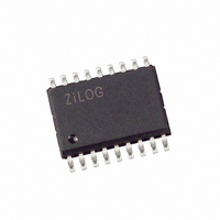
Z86E0208SSG1925 Zilog, Z86E0208SSG1925 Datasheet - Page 39

Z86E0208SSG1925
Manufacturer Part Number
Z86E0208SSG1925
Description
IC Z8 512 BYTE OTP 8MHZ 18-SOIC
Manufacturer
Zilog
Series
Z8®r
Datasheet
1.Z86E0208PSG1925.pdf
(60 pages)
Specifications of Z86E0208SSG1925
Core Processor
Z8
Core Size
8-Bit
Speed
8MHz
Peripherals
POR, WDT
Number Of I /o
14
Program Memory Size
512B (512 x 8)
Program Memory Type
OTP
Ram Size
61 x 8
Voltage - Supply (vcc/vdd)
3.5 V ~ 5.5 V
Oscillator Type
Internal
Operating Temperature
0°C ~ 70°C
Package / Case
18-SOIC (7.5mm Width)
Processor Series
Z86E02x
Core
Z8
Data Bus Width
8 bit
Data Ram Size
61 B
Maximum Clock Frequency
8 MHz
Number Of Programmable I/os
14
Number Of Timers
1
Operating Supply Voltage
4.5 V to 5.5 V
Maximum Operating Temperature
+ 70 C
Mounting Style
SMD/SMT
Minimum Operating Temperature
0 C
Lead Free Status / RoHS Status
Lead free / RoHS Compliant
Eeprom Size
-
Data Converters
-
Connectivity
-
Lead Free Status / Rohs Status
Details
PS014802-0903
Counter/Timer
Interrupts
T
IN
Clock
Logic
There is one 8-bit programmable counter/timer (T1), driven by its own 6-bit pro-
grammable prescaler. The T1 prescaler is driven by internal or external clock
sources (Figure 16).
The 6-bit prescaler divide the input frequency of the clock source by any integer
number from 1 to 64. Each prescaler drives its counter, which decrements the
value (1 to 256) that is loaded into the counter. When both counter and prescaler
reach the end of count, a timer interrupt request IRQ5 (T1) is generated.
The counter can be programmed to start, stop, restart to continue, or restart from
the initial value. The counters are also programmed to stop upon reaching zero
(SINGLE-PASS mode) or to automatically reload the initial value and continue
counting (MODULO-N CONTINUOUS mode).
The counter, but not the prescaler, are read at any time without disturbing their
value or count mode. The clock source for T1 is user-definable and is either the
internal microprocessor clock divided by four, or an external signal input through
Port 3. The TIMER mode register configures the external timer input (P31) as an
external clock, a trigger input that is retriggerable or non-retriggerable, or used as
a gate input for the internal clock.
The Z8
maskable and prioritized (Figure 17). The sources are divided as follows: the fall-
ing edge of P31 (AN 1), P32 (AN2), P33 (REF), the rising edge of P32 (AN2), by
software, and one counter/timer. The Interrupt Mask Register globally or individu-
ally enables or disables the six interrupt requests (Interrupt Types, Sources, and
Vectors).
P31
Internal Clock
Gated Clock
Triggered Clock
External Clock
®
4
features six interrupts from six different sources. These interrupts are
Figure 16. Counter/Timer Block Diagram
Write
Initial Value
Counter
Register
Down
PRE1
6-Bit
General-Purpose OTP MCU with 14 I/O Lines
Write
Internal Data Bus
Initial Value
Register
Counter
Down
8-Bit
T1
Read
Current Value
Register
T1
Z86E02 SL 1925
IRQ5
33


