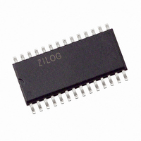
Z8F0412SJ020SG Zilog, Z8F0412SJ020SG Datasheet - Page 168

Z8F0412SJ020SG
Manufacturer Part Number
Z8F0412SJ020SG
Description
IC ENCORE MCU FLASH 4K 28SOIC
Manufacturer
Zilog
Series
Encore!® XP®r
Datasheet
1.Z8F08200100KIT.pdf
(264 pages)
Specifications of Z8F0412SJ020SG
Core Processor
Z8
Core Size
8-Bit
Speed
20MHz
Connectivity
I²C, IrDA, SPI, UART/USART
Peripherals
Brown-out Detect/Reset, POR, PWM, WDT
Number Of I /o
19
Program Memory Size
4KB (4K x 8)
Program Memory Type
FLASH
Ram Size
1K x 8
Voltage - Supply (vcc/vdd)
2.7 V ~ 3.6 V
Oscillator Type
Internal
Operating Temperature
0°C ~ 70°C
Package / Case
28-SOIC (7.5mm Width)
Processor Series
Z8F041xx
Core
eZ8
Data Bus Width
8 bit
Data Ram Size
1 KB
Interface Type
I2C, SPI, UART
Maximum Clock Frequency
20 MHz
Number Of Programmable I/os
19
Number Of Timers
2
Operating Supply Voltage
2.7 V to 3.6 V
Maximum Operating Temperature
+ 70 C
Mounting Style
SMD/SMT
Minimum Operating Temperature
0 C
Lead Free Status / RoHS Status
Lead free / RoHS Compliant
Eeprom Size
-
Data Converters
-
Lead Free Status / Rohs Status
Details
Other names
269-4107
Z8F0412SJ020SG
Z8F0412SJ020SG
Available stocks
Company
Part Number
Manufacturer
Quantity
Price
Part Number:
Z8F0412SJ020SG
Manufacturer:
ZILOG
Quantity:
20 000
- Current page: 168 of 264
- Download datasheet (6Mb)
Operation
PS022517-0508
Caution:
Timing Using the Flash Frequency Registers
Table 82. Z8 Encore! XP
The Flash Controller provides the proper signals and timing for Byte Programming, Page
Erase, and Mass Erase of the Flash memory. The Flash Controller contains a protection
mechanism, using the Flash Control Register (FCTL), to prevent accidental programming
or erasure. The following subsections provide details on the various operations (Lock,
Unlock, Sector Protect, Byte Programming, Page Erase, and Mass Erase).
Before performing a program or erase operation on the Flash memory, you must first
configure the Flash Frequency High and Low Byte registers. The Flash Frequency
registers allow programming and erasure of the Flash with system clock frequencies
ranging from 20 kHz through 20 MHz (the valid range is limited to the device operating
frequencies).
The Flash Frequency High and Low Byte registers combine to form a 16-bit value,
FFREQ, to control timing for Flash program and erase operations. The 16-bit Flash
Frequency value must contain the system clock frequency in kHz. This value is calculated
using the following equation:
FFREQ[15:0]
Flash Memory Address (Hex)
Flash programming and erasure are not supported for system clock fre-
quencies below 20 kHz, above 20 MHz, or outside of the device operating
frequency range. The Flash Frequency High and Low Byte registers must
be loaded with the correct value to insure proper Flash programming and
erase operations.
FE00H-FE3FH
FE54H-FFFFH
FE40H-FE53H
=
System Clock Frequency (Hz)
------------------------------------------------------------------------------ -
®
1000
F0822 Series Information Area Map
Function
Reserved
Part Number
20-character ASCII alphanumeric code
Left justified and filled with zeros
Reserved
Z8 Encore! XP
Product Specification
®
F0822 Series
Flash Memory
155
Related parts for Z8F0412SJ020SG
Image
Part Number
Description
Manufacturer
Datasheet
Request
R

Part Number:
Description:
Communication Controllers, ZILOG INTELLIGENT PERIPHERAL CONTROLLER (ZIP)
Manufacturer:
Zilog, Inc.
Datasheet:

Part Number:
Description:
KIT DEV FOR Z8 ENCORE 16K TO 64K
Manufacturer:
Zilog
Datasheet:

Part Number:
Description:
KIT DEV Z8 ENCORE XP 28-PIN
Manufacturer:
Zilog
Datasheet:

Part Number:
Description:
DEV KIT FOR Z8 ENCORE 8K/4K
Manufacturer:
Zilog
Datasheet:

Part Number:
Description:
KIT DEV Z8 ENCORE XP 28-PIN
Manufacturer:
Zilog
Datasheet:

Part Number:
Description:
DEV KIT FOR Z8 ENCORE 4K TO 8K
Manufacturer:
Zilog
Datasheet:

Part Number:
Description:
CMOS Z8 microcontroller. ROM 16 Kbytes, RAM 256 bytes, speed 16 MHz, 32 lines I/O, 3.0V to 5.5V
Manufacturer:
Zilog, Inc.
Datasheet:

Part Number:
Description:
Low-cost microcontroller. 512 bytes ROM, 61 bytes RAM, 8 MHz
Manufacturer:
Zilog, Inc.
Datasheet:

Part Number:
Description:
Z8 4K OTP Microcontroller
Manufacturer:
Zilog, Inc.
Datasheet:

Part Number:
Description:
CMOS SUPER8 ROMLESS MCU
Manufacturer:
Zilog, Inc.
Datasheet:

Part Number:
Description:
SL1866 CMOSZ8 OTP Microcontroller
Manufacturer:
Zilog, Inc.
Datasheet:

Part Number:
Description:
SL1866 CMOSZ8 OTP Microcontroller
Manufacturer:
Zilog, Inc.
Datasheet:

Part Number:
Description:
OTP (KB) = 1, RAM = 125, Speed = 12, I/O = 14, 8-bit Timers = 2, Comm Interfaces Other Features = Por, LV Protect, Voltage = 4.5-5.5V
Manufacturer:
Zilog, Inc.
Datasheet:

Part Number:
Description:
Manufacturer:
Zilog, Inc.
Datasheet:


